background image

Startup Sequence

www.ti.com

5

Startup Sequence

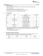
To activate the LM3269EVM Buck-Boost DC-DC converter output, execute the following steps:

1. Place EN pin LOW.

2. Power up PVIN (within the P

VIN

range of 2.7V to 5.5V).

3. Set VCON pin to 1/3 of desired output voltage (0.2

VCON

1.4V).

4. Place EN pin HIGH, then V

OUT

should present as expected.

6

List of Materials

Designator

Model

Description

Manufacturer

100

μ

F, optional , 6.3V, 1411 (3528)

CPVIN

(1)

Std

Std

Low ESR Tantalum

C1

(2)

Std

220 pF, optional, 01005 (0402)

Std

C2

(2)

Std

0.1

μ

F, optional, 0201 (0603)

TDK

C3

C1608X5R0J106K

10

μ

F, 6.3V, 0603 (1608)

C4

C1608X5R0J475K

4.7

μ

F, 6.3V, 0603 (1608)

Std

C5

(2)

Std

0.1

μ

F, optional, 0201 (0603)

Std

C6

(2)

Std

220 pF, optional, 01005 (0402)

Std

C7, C8

(3)

Std

0.47

μ

F, optional, 0201 (0603)

Std

C9

Std

Optional, 0402 (1005)

Std

L

MIPSZ2520D2R2

2.2

μ

H, 2.5 x 2.0 x 1.0 mm

FDK

R1

Std

Optional, 01005 (0402), Shorted

Std

U1

LM3269TLE

Buck-Boost Converter

Texas Instruments

(1)

CPVIN: The long test leads necessary for bench testing add significant parasitic inductances in series with the bench power
supply. The 100

μ

F capacitor at CPVIN reduces the impact that these parasitic inductances have on both static and transient

behavior during testing.

(2)

C1, C2, C5, C6 help to improve high frequency noise.

(3)

C7, C8 resemble PA decoupling capacitor.

7

Input/Output Capacitor Information

The total recommended actual capacitance on the VOUT bus should be at least 7.0

μ

F (4.7

μ

F + PA

decoupling caps) to take into account the DC bias degradation and other tolerances.

BUS

MIN (µF)

TYP (µF)

MAX (µF)

PVIN

10

VOUT

7

10

2

LM3269 Evaluation Board

SNVU162 – FEBRUARY 2013

Submit Documentation Feedback

Copyright © 2013, Texas Instruments Incorporated

Содержание LM3269

Страница 1: ... and electrical characteristics about the converter operation please refer to the LM3269 data sheet If you are considering using the LM3269 in a system design please review the PCB Layout Considerations section of the data sheet 2 Operating Conditions The device will operate under the following conditions VIN 2 7V VIN 5 5V Adjustable VOUT 0 6V to 4 2V VCON 0 2V to 1 4V VOUT equation VOUT 3 x VCON ...

Страница 2: ...0201 0603 Std C9 Std Optional 0402 1005 Std L MIPSZ2520D2R2 2 2 μH 2 5 x 2 0 x 1 0 mm FDK R1 Std Optional 01005 0402 Shorted Std U1 LM3269TLE Buck Boost Converter Texas Instruments 1 CPVIN The long test leads necessary for bench testing add significant parasitic inductances in series with the bench power supply The 100 μF capacitor at CPVIN reduces the impact that these parasitic inductances have ...

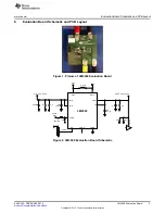
Страница 3: ...PA VIN R1 shorted C9 VCON input PVIN PVIN www ti com Evaluation Board Schematic and PCB Layout 8 Evaluation Board Schematic and PCB Layout Figure 1 Picture of LM3269 Evaluation Board Figure 2 LM3269 Evaluation Board Schematic 3 SNVU162 FEBRUARY 2013 LM3269 Evaluation Board Submit Documentation Feedback Copyright 2013 Texas Instruments Incorporated ...

Страница 4: ...d PCB Layout www ti com Figure 3 Top Layer Figure 4 Mid Layer 1 Figure 5 Mid Layer 2 Figure 6 Bottom Layer 4 LM3269 Evaluation Board SNVU162 FEBRUARY 2013 Submit Documentation Feedback Copyright 2013 Texas Instruments Incorporated ...
Страница 5: ... to D1 VOUT GND A2 NC Non connection Leave this pin floating do not connect to PVIN or PGND B2 EN Enable Pin Pulling this pin higher than 1 2V enables part to function C2 SGND Signal Ground for analog circuits and control circuitry D2 SW2 Switch pin for Internal Power Switches Connect inductor between SW1 and SW2 Power MOSFET input and power current input pin Optional low pass filtering may help b...

Страница 6: ...ency energy and has not been tested for compliance with the limits of computing devices pursuant to part 15 of FCC or ICES 003 rules which are designed to provide reasonable protection against radio frequency interference Operation of the equipment may cause interference with radio communications in which case the user at his own expense will be required to take whatever measures may be required t...

Страница 7: ... its gain should be so chosen that the equivalent isotropically radiated power e i r p is not more than that necessary for successful communication This radio transmitter has been approved by Industry Canada to operate with the antenna types listed in the user guide with the maximum permissible gain and required antenna impedance for each antenna type indicated Antenna types not included in this l...

Страница 8: ...er you obtained the Technical Regulations Conformity Certification as provided in Radio Law of Japan with respect to this product Also please do not transfer this product unless you give the same notice above to the transferee Please note that if you could not follow the instructions above you will be subject to penalties of Radio Law of Japan Texas Instruments Japan Limited address 24 1 Nishi Shi...

Страница 9: ... property damage personal injury or death If there are questions concerning these ratings please contact a TI field representative prior to connecting interface electronics including input power and intended loads Any loads applied outside of the specified output range may result in unintended and or inaccurate operation and or possible permanent damage to the EVM and or interface electronics Plea...

Страница 10: ...esponsible for compliance with all legal regulatory and safety related requirements concerning its products and any use of TI components in its applications notwithstanding any applications related information or support that may be provided by TI Buyer represents and agrees that it has all the necessary expertise to create and implement safeguards which anticipate dangerous consequences of failur...

Отзывы: