background image

6 EVM Schematic and PCB

The ISO1644DW isolated I

2

C EVM comes with an ISO1644DW installed in place of U1. This EVM can also

be configured for use with an ISO1642DW or ISO1643DW. Each signal line (SDAx, SCLx) is configured with a
3.3-kΩ pullup resistor (R1 to R4) to the corresponding power supply (VCCx). These resistors may be replaced
with 0805 resistors of other values per the application requirements. For insight on calculating appropriate pullup
resistor values for I

2

C buses, please refer to the 

I2C Bus Pullup Resistor Calculation

 application report

.

Note

ISO164x devices are designed to sink different amounts of current on side 1 and side 2, be careful to
choose resistors that keep I

OL1

 and I

OL2

 within the recommended operating range if replacing resistors

R1 to R4.

Signal pins may be tied directly to ground using the header pins (J1 on side 1; J2 on side 2) to simulate a
device pulling the I

2

C line low. While not being actively driven low, the lines will be pulled up through the included

pullup resistors. 

Signal lines should not be tied directly to a supply voltage without a pullup resistor to

limit input current

. These jumpers also provide input /output signal access, including for oscilloscope probes, to

each pin.

Note

Ensure that SDAx and SCLx signal lines are not tied directly to VCCx. A current-limiting pullup resistor
is required, and populated by default, to limit current in the cases where the device pins drive a
low-voltage.

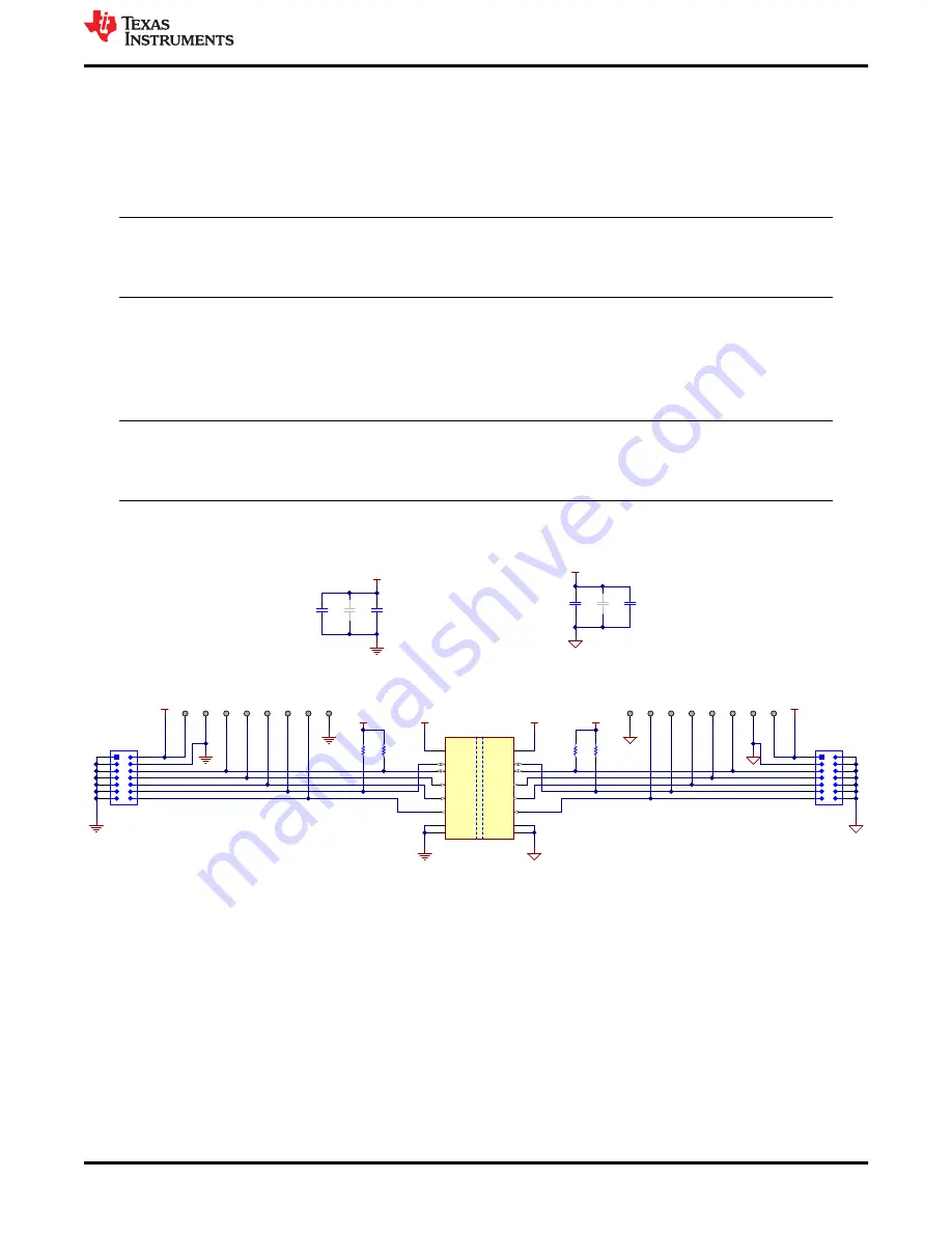
Figure 6-1

 shows the schematic diagram for this EVM, and 

Figure 6-2

 and 

Figure 6-3

 show the printed circuit

board (PCB) layout.

GND1

VCC1

100nF

C3

GND2

VCC2

100nF

C6

VCC1

GND1

GND2

VCC2

1µF

C2

DNP

1µF

C5

DNP

1

2

3

4

5

6

7

8

9

10

11

12

13

14

J1

1

2

3

4

5

6

7

8

9

10

11

12

13

14

J2

GND1

GND1

GND2

GND2

GND1

VCC1

VCC2

GND2

10uF

C1

10uF

C4

ISO1644DWR

VCC1

1

VCC2

16

SDA1

3

SDA2

14

SCL1

6

SCL2

11

INA

4

INB

5

INC

10

OUTA

13

OUTB

12

OUTC

7

GND1

2

GND1

8

GND2

9

GND2

15

U1

3.3k

R1

3.3k

R2

3.3k

R3

3.3k

R4

VCC1

VCC2

TP8

TP9

TP10

TP11

TP12

TP13

TP14

TP15

TP16

TP1

TP2

TP3

TP4

TP5

TP6

TP7

Figure 6-1. ISO1644DWEVM Schematic

www.ti.com

EVM Schematic and PCB

SLLU329 – JUNE 2021

Submit Document Feedback

ISO1644DWEVM Reinforced Isolated I

2

C With GPIOs Evaluation Module

5

Copyright © 2021 Texas Instruments Incorporated

Содержание ISO1644DWEVM

Страница 1: ...olated I2C Transceivers With GPIO 3 4 EVM Setup and Operation 4 5 Bill of Materials 4 6 EVM Schematic and PCB 5 List of Figures Figure 3 1 ISO1642 ISO1643 and ISO1644 Pinouts 3 Figure 3 2 ISO1644DWEVM Top View 3 Figure 4 1 Basic ISO1644DWEVM Operation 4 Figure 6 1 ISO1644DWEVM Schematic 5 Figure 6 2 ISO1644DWEVM Top PCB Layout 6 Figure 6 3 ISO1644DWEVM Bottom PCB Layout 6 List of Tables Table 5 1 ...

Страница 2: ...damaging sensitive circuitry ISO1642 ISO1643 and ISO1644 devices have two bidirectional data channels for I2C clock and data lines and are fit for multi master or clock stretching applications These devices achieve isolated bidirectional communication by introducing a static voltage offset SVO making the side 1 low level output greater than the side 1 low level input thus preventing an internal lo...

Страница 3: ... SDA1 SDA2 Isolation 16 15 14 13 9 10 11 12 1 2 3 4 8 7 6 5 INA INB GND1 OUT C GND2 OUTB OUTA INC ISO1644DW Figure 3 1 ISO1642 ISO1643 and ISO1644 Pinouts The EVM PCB is shown in Figure 3 2 and comes with an ISO1644DW installed in place of U1 However this EVM can also be configured for evaluation of ISO1642DW and ISO1643DW by replacing the included ISO1644DW device in place of U1 Figure 3 2 ISO164...

Страница 4: ...5 INA INB GND1 OUTC GND2 OUTB OUTA INC ISO1644DW Figure 4 1 Basic ISO1644DWEVM Operation Although the ISO1642 ISO1643 and ISO1644 devices feature bidirectional data channels the devices perform optimally when side 1 SDA1 and SCL1 is connected to a single controller or node of an I2C network while side 2 SDA2 and SCL2 is connected to the I2C bus Please note that bidirectional clocks can be used on ...

Страница 5: ...s should not be tied directly to a supply voltage without a pullup resistor to limit input current These jumpers also provide input output signal access including for oscilloscope probes to each pin Note Ensure that SDAx and SCLx signal lines are not tied directly to VCCx A current limiting pullup resistor is required and populated by default to limit current in the cases where the device pins dri...

Страница 6: ...yout Figure 6 3 ISO1644DWEVM Bottom PCB Layout EVM Schematic and PCB www ti com 6 ISO1644DWEVM Reinforced Isolated I2C With GPIOs Evaluation Module SLLU329 JUNE 2021 Submit Document Feedback Copyright 2021 Texas Instruments Incorporated ...

Страница 7: ...other than TI b the nonconformity resulted from User s design specifications or instructions for such EVMs or improper system design or c User has not paid on time Testing and other quality control techniques are used to the extent TI deems necessary TI does not test all parameters of each EVM User s claims against TI under this Section 2 are void if User fails to notify TI of any apparent defects...

Страница 8: ... These limits are designed to provide reasonable protection against harmful interference in a residential installation This equipment generates uses and can radiate radio frequency energy and if not installed and used in accordance with the instructions may cause harmful interference to radio communications However there is no guarantee that interference will not occur in a particular installation...

Страница 9: ...y for convenience and should be verified by User 1 Use EVMs in a shielded room or any other test facility as defined in the notification 173 issued by Ministry of Internal Affairs and Communications on March 28 2006 based on Sub section 1 1 of Article 6 of the Ministry s Rule for Enforcement of Radio Law of Japan 2 Use EVMs only after User obtains the license of Test Radio Station as provided in R...

Страница 10: ... any interfaces electronic and or mechanical between the EVM and any human body are designed with suitable isolation and means to safely limit accessible leakage currents to minimize the risk of electrical shock hazard User assumes all responsibility and liability for any improper or unsafe handling or use of the EVM by User or its employees affiliates contractors or designees 4 4 User assumes all...

Страница 11: ...OR DAMAGES ARE CLAIMED THE EXISTENCE OF MORE THAN ONE CLAIM SHALL NOT ENLARGE OR EXTEND THIS LIMIT 9 Return Policy Except as otherwise provided TI does not offer any refunds returns or exchanges Furthermore no return of EVM s will be accepted if the package has been opened and no return of the EVM s will be accepted if they are damaged or otherwise not in a resalable condition If User feels it has...

Страница 12: ...s are subject to change without notice TI grants you permission to use these resources only for development of an application that uses the TI products described in the resource Other reproduction and display of these resources is prohibited No license is granted to any other TI intellectual property right or to any third party intellectual property right TI disclaims responsibility for and you wi...

Отзывы: