


Introduction
www.ti.com
2
SLUUBL3A – June 2017 – Revised October 2017
Submit Documentation Feedback
Copyright © 2017, Texas Instruments Incorporated
bq25606 PWR772 Evaluation Module
1
Introduction
1.1
EVM Features
For detailed features and operation, refer to
Table 1
for a list of devices and their data sheets.
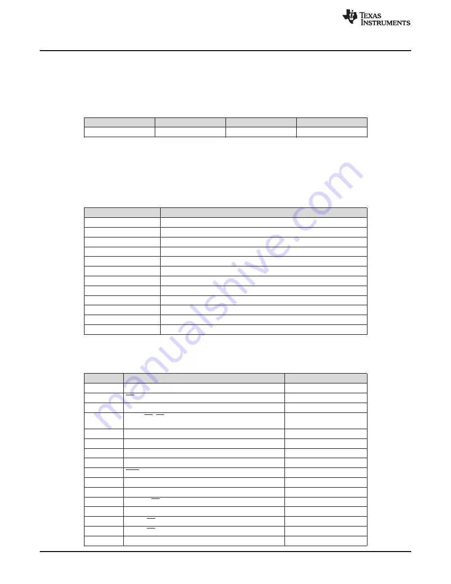
Table 1. Device Data Sheets
Device
Data Sheet
EVM Label
Variant
bq25606
SLUSCK6
BQ25606EVM-772
004
The bq25606 evaluation module (EVM) is a standalone charger module without I
2
C control.
1.2
I/O Descriptions
Table 2
lists the jumper connections available on this EVM.
Table 2. EVM Connections
Jack
Description
J1-VAC
Input positive terminal
J1-GND
Ground Input: negative terminal (ground terminal)
J2-PMID
PMID pin connection
J2-GND
Ground
J3
Output mini-USB port
J4-SYS
Connected to system
J4-GND
Ground
J5-BATSNS_ICHG
BATSNS or ICHG pin connection
J5-BAT
Connected to battery pack positive node
J5-GND
Ground
J6
I2C 4-pin connector
J7
USB-TO-GPIO connector (Not populated)
Table 3
lists the EVM jumper connections.
Table 3. EVM Jumper Connections and Shunt Installation
Jack
Description
bq25606 Setting
JP1
PSEL pin selection
Not installed
JP2
CE pin setting: pull low to enable the charge
Installed
JP3
OTG pin setting: pull high to enable OTG mode
Short OTG to GND
JP4
STAT, PG, CE, INT, and OTG pins pullup source (SYS or
BAT)
Short to SYS
JP5
TS pin to GND
Not installed
JP6
TS resistor divider pullup source (REGN) connection
Installed
JP7
Internal 10 k
Ω
to GND to TS pin
Installed
JP8
BATSNS selection
Not installed
JP9
QON and VSET pin setting
Not installed
JP10
STAT pin setting
Installed
JP11
Add SYS cap
Not installed
JP12
SDA and PG pin setting
Installed
JP13
D+ and PSEL to J3
Not Installed
JP14
D– and PG to J3
Not Installed
JP15
D– and PG pin setting
Not installed
JP16
Add VBUS cap
Not installed