


TXMC638 User Manual Issue 1.0.2
Page 44 of 86
7.8.2 SPI-Flash
The TXMC638 provides a Micron N25Q128A 128-Mbit serial Flash memory. This Flash is used as FPGA
configuration source (default configuration source).
After configuration, it is always accessible from the FPGA, so it also can be used for code or user data
storage.
The SPI-EEPROM is connected via Quad (x4) SPI interface to the User FPGA (Kintex-7) configuration
interface.
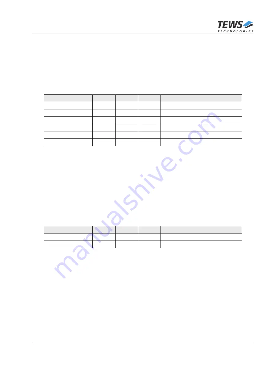
SPI-PROM Signal
Bank
V
CCO
Pin
Description / Kintex-7
CLK
14
3.3V
C8
Serial Clock (CCLK_B)
CS#
14
3.3V
C23
Chip Select (FCS_B)
DI (bit0)
14
3.3V
B24
Serial Data input (MOSI) / MISO[0]
DO (bit1)
14
3.3V
A25
Serial Data output (DIN) / MISO[1]
WP# (bit2)
14
3.3V
B22
MISO[2] – D02
HOLD# (bit3)
14
3.3V
A22
MISO[3] – D03
Table 7-9 : FPGA SPI-Flash Connections
7.8.3 I2C - EEPROM
The TXMC638 provides an Atmel AT24C04D (512x8) I2C-Compatible (2-wire) Serial EEPROM.
This EEPROM is used as ADC calibration data source. During factory test the analog input channel gain
error and offset error are determined. For each device a 16 bit correction value is stored to the I2C
EEPROM. These calibration data have been determined with TEWS test environment and build such a
possible basis. If system specific calibration data are needed, the calibration of the entire system can be
done by user and the I2C EEPROM could be used as a possible memory.
The I2C EEPROM is connected via 2-wire interface to User FPGA (Kintex-7). As usual for the I2C interface
the two pins must be realized as open drain buffer.
SPI-PROM Signal
Bank
V
CCO
Pin
Description / Kintex-7
FPGA_SCL
14
3.3V
F25
Serial clock
FPGA_SDA
14
3.3V
G26
Serial data
Table 7-10: FPGA I2C EEPROM Connections
For using the serial I2C interface between the USER FPGA (Kintex-7) and the I2C EEPROM please see the
Atmel AT24C04D data sheet which describes the serial communication process.
7.8.3.1 I2C Calibration Data
There are two errors affecting the accuracy of the ADC that can be corrected using the factory calibrated
calibration data. The correction values are obtained during factory calibration and are stored in an on-board
I2C EEPROM as 2-complement 16 bit values in the range from -32768 to +32767. To achieve a higher
accuracy, they are scaled to ¼LSB.
ADC Offset Error:
The offset error is the data value when converting with the input connected to its own ground in single-ended
mode, or with shorted inputs in differential mode. This error is corrected by subtracting the known error from
the reading.


