8
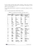
The PCIe interface pins PETpx, PETnx, PERpx, and PERnx are named with the following
convention: “PE” stands for PCIe high speed, “T” for Transmitter, “R” for Receiver, “p” for
positive (+), and “n” for negative (-).
Note that adjacent differential pairs are separated by two ground pins to manage the connector
crosstalk.
Table 3-1
gives the wiring information of the PCIe Edge connector.
Table 3-1
Pin assignments and descriptions on PCIe Edge connector
Pin Numbers
Side B
Side A
Name
Description
Name
Description
1
NC
NC
PRSNT1n
Hot-Plug
presence detect
2
NC
NC
NC
NC
3
NC
NC
NC
NC
4
GND
Ground
GND
Ground
5
NC
NC
NC
NC
6
NC
NC
NC
NC
7
GND
Ground
NC
NC
8
VCC3P3
3.3V Power
NC
NC
9
NC
NC
VCC3P3
3.3V Power
10
3.3VAUX
3.3 V Auxiliary
Power
VCC3P3
3.3V Power
11
WAKE
NC
PERSTn
Fundamental
Reset
Mechanical Key
12
RSVD
Reserved
GND
Ground
13
GND
Ground
Reference clock
(differential
pair)
14
PETp0
Transmitter
differential pair,
Lane 0
REFCLK-
15
PETn0
GND
Ground
16
GND
Ground
PERp0
Receiver
differential pair,
Lane 0
17
PRSNT2n
Hot-Plug
presence detect
PERn0
18
GND
Ground
GND
Ground
19
PETp1
Transmitter
differential pair,
Lane 1
20
PETn1
GND
Ground
21
GND
Ground
PERp1
Receiver
differential pair,
Lane 1
22
GND
Ground
PERn1
23
PETp2
Transmitter
differential pair,
GND
Ground
24
PETn2
GND
Ground
Содержание PCA
Страница 1: ......
Страница 7: ...6 Figure 2 3 Block Diagram of PCA ...


