Telink FR1 PCB Design Guideline
AN-22051900-E1 Ver. 1.0.0
7
2.
Application Board Structure ID
According to the complexity of the components, taking into account cost and the difficulty of routing, the the
PCB design for Telink chips can be divided into single-layer boards or double-layer boards.
2.1
Single-layer board
In single-layer board design, make sure that all components and keys can be placed on the same side and
there should be enough space for the PCB antenna. This is suitable for boards with a small number of
components and routings.
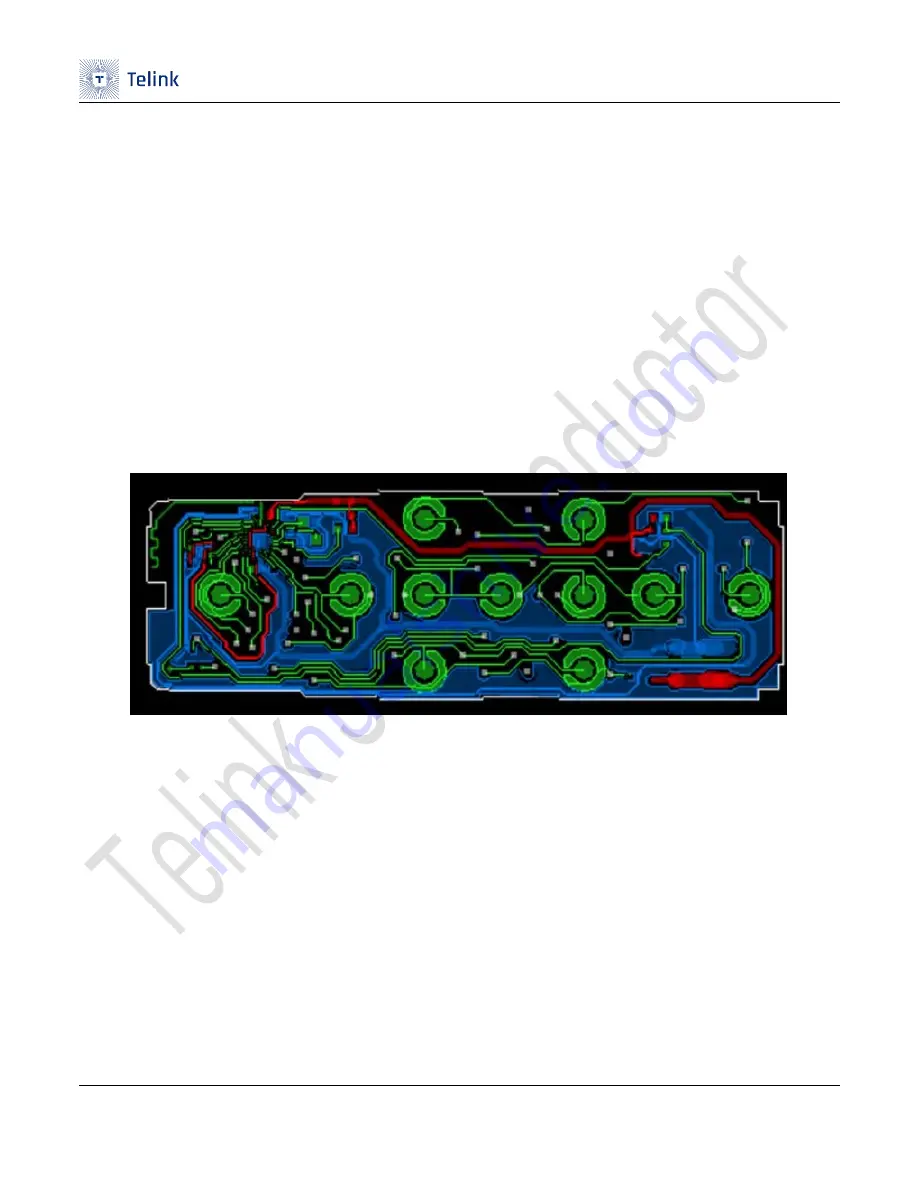
The remote control board shown below can be designed as a single-layer board.
Figure 2-1 Single-layer board


