Teknor Industrial Computers VIPer808 Скачать руководство пользователя страница 108

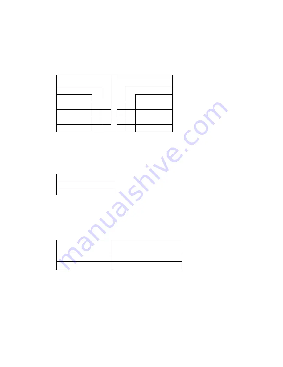
       Connector Pinouts       D-11

Ethernet  10 Base-T  RJ45 Connector (J14) - Pinout

Error! Bookmark not

defined.Pin Number

Pin Number

Signal Flow

Signal Flow

Signal

Signal

TXD+

O

1

5

-

Not Connected

TXD-

O

2

6

I

RXD-

RXD+

I

3

7

-

Not Connected

Not Connected

-

4

8

-

Not Connected

Ethernet  10 Base-2 
BNC Connector (J15) - Pinout

Signal Name

Center Conductor

Shield

The Ethernet 10 Base-2 connector is a standard BNC connector.

Suspend / Resume Momentary Switch (J16) - Pinout

Error! Bookmark not
defined.Pin Number

Signal

1

VCC (+5V)

2

SWITCH

Содержание VIPer808

Страница 1: ...VERSION 1 2 MARCH 1997 TEKNOR INDUSTRIAL COMPUTERS INC 616 Cure Boivin Boisbriand Quebec J7G 2A7 CANADA NOTE This manual is for reference purposes only Reproduction in whole or in part is authorized...

Страница 2: ...of information or the use of products described herein This document may contain information or refer to products protected by the copyrights or patents of others and does not convey any license under...

Страница 3: ...1 01 GETTING STARTED 1 1 1 02 HOW THE BOARD CAN BE USED 1 2 1 03 IMPORTANT PRECAUTIONS WHEN WORKING WITH A BOARD 1 3 1 04 UNPACKING 1 4 SECTION 2 INSTALLING MEMORY 2 1 2 01 TYPES OF MEMORY ON BOARD 2...

Страница 4: ...T LED 4 6 4 05 PC 104 EXPANSION CARDS 4 7 4 06 PS 2 MOUSE 4 7 SECTION 5 INSTALLING PERIPHERALS PARALLEL SERIAL ETHERNET 5 1 5 01 PARALLEL PORT 5 1 5 02 SERIAL PORTS 5 6 5 03 ETHERNET PORT 5 10 SECTION...

Страница 5: ...SOURCE 8 1 8 02 POWER MANAGEMENT MODES 8 2 8 03 RESET CIRCUIT 8 3 8 04 POWER FAIL DETECTION CIRCUIT 8 4 8 05 WATCHDOG TIMER 8 6 SECTION 9 VIPer SOFTWARE SETUP 9 1 9 01 AMIBIOS SETUP PROGRAM 9 2 9 02...

Страница 6: ...TING INDUSTRY STANDARDS A 6 APPENDIX B MEMORY I O MAPS B 1 B 01 MEMORY MAPS B 1 B 02 I O MAPS B 3 APPENDIX C MECHANICAL LAYOUT BLOCK DIAGRAM C 1 APPENDIX D CONNECTOR PINOUTS D 1 APPENDIX E RECOMMENDED...

Страница 7: ...3 2 2 Assembly Bottom 2 5 3 1 VIPer808 Jumper Locations with Default Settings 3 3 6 1 Floppy Disk Cable 6 7 7 1 VIPer808 Connector Locations 7 3 B 1 Memory Map Diagram B 1 C 1 Mechanical Specificatio...

Страница 8: ...W15C 3 10 3 1f Jumper Settings W18 W20 W23 3 11 4 1 8237 DMA Controllers 4 4 4 2 8259 Interrupt Controllers 4 5 4 3 Keyboard Speaker Connector J3 4 6 5 1 Printer Parallel Port J13 Standard Mode 5 2 5...

Страница 9: ...out 7 2 8 1 External Power Connector J9 Pinout 8 1 9 1 Advanced Setup 9 9 9 2 Chipset Setup 9 11 9 3 Power Management Setup 9 11 9 4 PCI PnP Setup 9 13 9 5 Peripheral Setup 9 13 A 1 Maximum Operating...

Страница 10: ...les the battery is not installed when you receive the board If you need a jumper cap we suggest you use the one on the Watchdog Timer jumper since it is rarely needed if you wish to purchase jumper ca...

Страница 11: ...2 running at 66 MHz 5V Intel 486DX4 running at 100 MHz 3 3V SGS 486DX2V running at 66 MHz 3 3V SGS 486DX4V running at 100 MHz 3 3V Each microprocessor has Internal Cache Memory The VIPer808 board supp...

Страница 12: ...VIPer808 includes a local bus IDE hard disk interface for a high performance disk subsystem The VIPer808 includes an enhanced super Floppy Controller which supports two Floppy Disk Drives of up to 2...

Страница 13: ...iew of the VIPer808 board plus installation and setup procedures A topical index of these Sections is included below TOPICS SECTIONS Cable connections 5 6 and 7 Cache 4 CPUs 4 CRT screen 7 Ethernet 5...

Страница 14: ...08 SPECIFICATIONS Appendix B MEMORY I O MAPS Appendix C MECHANICAL LAYOUT BLOCK DIAGRAM Appendix D CONNECTOR PINOUTS Appendix E RECOMMENDED DEVICES MATING CONNECTORS Appendix F ERROR CODES At the end...

Страница 15: ...NSTALLING MEMORY SECTION 3 SETTING JUMPERS SECTION 4 INSTALLING WORKING WITH SYSTEM COMPONENTS SECTION 5 INSTALLING PERIPHERALS PARALLEL SERIAL ETHERNET SECTION 6 INSTALLING IDE FLOPPY DEVICES SECTION...

Страница 16: ...g the connectors and jumpers of the board and understanding how the board can be configured via the jumpers Then they can consult the TABLE OF CONTENTS at the beginning of this manual for specific inf...

Страница 17: ...an be used as a single board computer in conjunction with a passive backplane Power is drawn directly from the AT bus The VIPer808 can be used as part of a stand alone system with no backplane The boa...

Страница 18: ...until you are ready to install it Touch a grounded surface before removing the board from its package or wear a grounding wrist strap this will discharge any static electricity that may have built up...

Страница 19: ...tic Electricity Precautions in section 1 03 1 Open the box remove the board from its antistatic wrapping and place it on a grounded surface Inspect the board for damage If there is any damage or items...

Страница 20: ...the only type of memory which can be installed by the user See section 2 02 for instructions on installing SIMMs The location of the two 72 pin vertical SIMM sockets appears on Diagram 2 1 and are la...

Страница 21: ...Installing Memory 2 3 DIAGRAM 2 1 Assembly Top...

Страница 22: ...Installing Memory 2 5 DIAGRAM 2 2 Assembly Bottom...

Страница 23: ...4MB modules will be available Consult the table on the following page to see which SIMM configurations are available on the VIPer808 DRAM devices with page mode at 70ns maximum access time is recommen...

Страница 24: ...6 2MB 512Kx36 3MB 2MB 512Kx36 1MB 256Kx36 4MB 2MB 512Kx36 2MB 512Kx36 4MB 4MB 1Mx36 4MB 4MB 1Mx36 8MB 4MB 1Mx36 4MB 1Mx36 8MB 8MB 2Mx36 8MB 8MB 2Mx36 12MB 4MB 1Mx36 8MB 2Mx36 12MB 8MB 2Mx36 4MB 1Mx36...

Страница 25: ...close a jumper by placing a plastic jumper cap over two pins of the jumper switch and you open a jumper switch by removing a jumper cap 3 02 JUMPER LOCATIONS ON THE BOARD Diagram 3 1 on the next page...

Страница 26: ...Setting Jumpers 3 3 DIAGRAM 3 1 VIPer808 Jumper Locations with Default Settings...

Страница 27: ...Setting Jumpers 3 5 3 03 JUMPER SETTINGS Table 3 1a to 3 1f on the following pages 3 6 to 3 11 show the jumper settings...

Страница 28: ...Setting Jumpers 3 6 TABLE 3 1a Jumper Settings W1 W4 W13 W14...

Страница 29: ...Setting Jumpers 3 7 TABLE 3 1b AMD DX2 DX4 CPU Jumper Settings W1 W15 W15C...

Страница 30: ...Setting Jumpers 3 8 TABLE 3 1c AMD 5x86 CPU Jumper Settings W1 W15 W15C...

Страница 31: ...Setting Jumpers 3 9 TABLE 3 1d Intel CPU Jumper Settings W1 W15 W15C...

Страница 32: ...Setting Jumpers 3 10 TABLE 3 1e SGS CPU Jumper Settings W1 W15 W15C...

Страница 33: ...Setting Jumpers 3 11 TABLE 3 1f Jumper Settings W18 W20 W23...

Страница 34: ...Intel 486DX4 running at 100 MHz 3 3V SGS 486DX2V running at 66 MHz 3 3V SGS 486DX4V running at 100 MHz 3 3V The Math Co processor is internal to the CPU Central Processing Unit The above processors a...

Страница 35: ...lf the maximum CPU internal clock speed or less For DX4 microprocessors external bus speed is set to one third the maximum CPU internal clock speed or less For 5x86 microprocessors external bus speed...

Страница 36: ...the CPU retrieves data from Cache a Cache hit occurs On the other hand when the CPU must access data from System Memory a Cache miss occurs Internal Cache Memory is enabled or disabled in the Advanced...

Страница 37: ...Clock and Reset Interface a Local Bus IDE Drive Interface for high performance disk subsystem and integrated 82C206 functions The System Controller is 100 IBM PC AT compatible It includes three 8254 C...

Страница 38: ...rupt Controllers CONTROLLER 1 CONTROLLER 2 IRQ 0 Timer 0 IRQ 8 Real time clock IRQ 1 Keyboard IRQ 9 Available Ethernet IRQ 2 Cascade controller 2 IRQ 10 Available IRQ 3 COM 2 IRQ 11 Available IRQ 4 CO...

Страница 39: ...5 6 VCC 5V SPKR O 7 8 VCC 5V KBDINH I 9 10 GND Not Connected 11 12 GND PBRES I 13 14 GND HDD ACTIVE O 15 16 VCC 5V Active low signal The following functions are available on the connector Speaker An...

Страница 40: ...104 are already offered by over 70 companies If you require additional information on the PC 104 standard please contact our Technical Support department 4 06 PS 2 MOUSE The board supports a mouse thr...

Страница 41: ...RALLEL SERIAL ETHERNET 5 01 PARALLEL PORT 5 01 1 MODES The parallel port is a multi mode parallel port supporting the following modes Standard Parallel Port SPP This mode is IBM XT AT compatible and P...

Страница 42: ...or this connector when it is in Standard mode TABLE 5 1 Printer Parallel Port J13 Standard Mode Pin Number Pin Number Signal Flow Signal Flow Signal Signal STROBE O 1 2 O AUTOFD D0 I O 3 4 I ERROR D1...

Страница 43: ...r Parallel Port J13 EPP Mode Pin Number Pin Number Signal Flow Signal Flow Signal Signal WRITE O 1 2 O DATASTB D0 I O 3 4 Not Used D1 I O 5 6 Not Used D2 I O 7 8 O ADDRSTRB D3 I O 9 10 GND D4 I O 11 1...

Страница 44: ...D1 I O 5 6 O INIT 1 REVERSERQST 3 D2 I O 7 8 O SELECTIN 1 3 D3 I O 9 10 GND D4 I O 11 12 GND D5 I O 13 14 GND D6 I O 15 16 GND D7 I O 17 18 GND ACK I 19 20 GND BUSY PERIPHACK3 I 21 22 GND PERROR ACKRE...

Страница 45: ...om the AMIBIOS Setup program s main menu From the Setup window select the Peripheral icon In the Peripheral Setup screen these options may be set ONBOARD PARALLEL PORT PARALLEL PORT IRQ PARALLEL PORT...

Страница 46: ...Installing Peripherals Parallel Serial Ethernet 5 6 5 02 SERIAL PORTS There are two 16550 compatible serial ports These have internal 16 byte FIFO buffers for more efficient data transfers...

Страница 47: ...ected TABLE 5 4b IBM 9 Pin DSUB Standard Pin Number Pin Number Signal Flow Signal Flow Signal Signal DCD I 1 2 I RX TX I 3 4 O DTR GND 5 6 I DSR RTS O 7 8 I CTS RI I 9 TEKNOR offers a 10 pin header to...

Страница 48: ...LE 5 5b IBM 9 Pin DSUB Standard Pin Number Pin Number Signal Flow Signal Flow Signal Signal DCD I 1 2 I RX TX I 3 4 O DTR GND 5 6 I DSR RTS O 7 8 I CTS RI I 9 TEKNOR offers a 10 pin header to 9 pin DS...

Страница 49: ...ollow these steps from the AMIBIOS Setup program s main menu From the Setup window select the Peripheral icon In the Peripheral Setup screen these options may be set ONBOARD SERIAL PORT 1 and ONBOARD...

Страница 50: ...em overhead providing sufficient latency during packet transmission and reception and minimizing intervention during normal network error recovery Supports Microsoft s Plug and Play System configurati...

Страница 51: ...You must refer to the READ_NET TXT ASCII or READ_NET DOC WORD 6 0 file also on the diskette for instructions on installing the drivers Once the proper Ethernet driver is installed the onboard Plug and...

Страница 52: ...nector appears in Table 5 7 TABLE 5 6 Ethernet 10 Base T RJ45 Connector J14 Pinout Pin Number Pin Number Signal Flow Signal Flow Signal Signal TXD O 1 5 Not Connected TXD O 2 6 I RXD RXD I 3 7 Not Con...

Страница 53: ...ted Disk Drives The AT embedded drive architecture incorporates drive electronics and controller circuitry on a single printed circuit board which is mounted directly to the disk drive chassis The int...

Страница 54: ...34 36 38 40 I O I O I O I O I O I O I O I O I O I I GND HD8 HD9 HD10 HD11 HD12 HD13 HD14 HD15 Not Connected GND GND GND BALE GND IOCS16 Not Connected SA2 CS1 GND Active low signal 6 01 3 IDE HOOK UP F...

Страница 55: ...01 4 IDE JUMPER IDE Controller jumper and its setting appears below W14 IOCHRDY signal to IDE interface Shorted Enabled Or open Disabled This is the initial setting For location and setting of jumper...

Страница 56: ...parameters for that hard disk You should check your hard disk data sheets to know if any of the other options LBA LARGE MODE BLOCK MODE and 32BIT MODE should be set to ON if your hard disk supports t...

Страница 57: ...TYPES OF FLOPPY DEVICES SUPPORTED The floppy disk controller is IBM PC XT AT compatible single and double density and supports Enhanced Floppy Mode 2 88MB It handles 3 5 inch and 5 25 inch low and hi...

Страница 58: ...GND GND GND GND GND GND Not Connected GND GND GND GND Not Connected Not Connected GND Not Connected 2 4 6 8 10 12 14 16 18 20 22 24 26 28 30 32 34 O I O O O O O O O O I I I O I DRV DENS SEL 0 Not Conn...

Страница 59: ...lation of the floppy drives is done via a standard IBM 34 pin flat ribbon cable that connects to J2 DIAGRAM 6 1 Floppy Disk Cable Enhanced Floppy Mode In order to connect your 2 88MB floppy drive simp...

Страница 60: ...een select the Floppy A icon or the Floppy B icon The settings are 360KB 5 inch 1 2MB 5 inch 720KB 3 inch 1 44MB 3 inch or 2 88MB 3 inch Return to the main menu and select the Peripheral icon from the...

Страница 61: ...level 7 01 1 CRT SUPPORT The video controller supports both monochrome and color VGA SVGA displays with resolution of up to 1280 x 1024 256 colors However since the video controller outputs only anal...

Страница 62: ...female connector See Diagram 7 1 on the following page for the location of J12 7 02 1 SVGA CONNECTOR J12 The VGA connector s pinout appears in Table 7 1 TABLE 7 1 SVGA Connector J12 Pinout Pin Number...

Страница 63: ...ems are powered from an outside power supply through the J9 connector ISA AT bus When the board is in a passive backplane system it is powered through the ISA bus The pinout for the J9 power connector...

Страница 64: ...t Setup screen Each mode is described below 8 02 1 DOZE MODE The Doze Mode is the System Controller s first level of power conservation During Doze Mode the display and hard drive will remain active I...

Страница 65: ...s an easy and effective way of resetting the system See Section 4 04 for more information 8 03 2 ONBOARD POWER DETECTION An onboard device which is part of the reset circuit constantly monitors the vo...

Страница 66: ...user or the system If the W21 jumper is left open no NMI is generated however an algorithm could be used to detect a low battery condition and respond accordingly An example of such an user defined pr...

Страница 67: ...is connected to the input of the power fail circuit which has its threshold set to 1 25V R98 can be calculated as follows R98 1K VI 1 25 where VI is input voltage on pin 6 1 25 of the power connector...

Страница 68: ...R 0x26 word Data outport INDEXREGISTER 0x111 Set bit 15 of Select Register to Low Data inport DATAREGISTER that sets the GPIO3 pin to Enabled Data Data 0x8000 Mask on bit 15 outport INDEXREGISTER 0x11...

Страница 69: ...ed changes the timeout to 100 ms Shorting R165 and installing a capacitor at C173 will change the timeout period according to the following formulae Timeout milliseconds 400 47pF C or C173 Timeout mil...

Страница 70: ...are configurable The setup program allows for minimal hardware configuration The AMIBIOS Setup program which is used to change operating parameters is explained in section 9 01 The procedure for updat...

Страница 71: ...en the operating system and the hardware of the VIPer808 single board computer The interface provided by AMIBIOS is 100 IBM AT compatible All functions accept similar inputs as IBM and provide the sam...

Страница 72: ...ed above meaning that you can select items in that window To highlight the other windows press the TAB key on the keyboard or if a supported mouse1 was detected move the arrow cursor over the desired...

Страница 73: ...g one of the arrow keys to highlight the desired item then by pressing the ENTER key or by clicking the mouse over the desired selection The windows in the program have layers like boxes inside boxes...

Страница 74: ...you can save the configuration in CMOS RAM by selecting this option After the information is saved the computer is automatically rebooted This option will not change the default values saved in Boot...

Страница 75: ...parameters and floppy drives Advanced Setup handles options and features such as key repetition settings boot sequence NUM LOCK and password checking shadowing Chipset Setup sets chipset specific opt...

Страница 76: ...a sheets to know if any of the other options LBA LARGE MODE BLOCK MODE and 32BIT MODE should be set to ON if your hard disk supports these modes enabling them will optimize your system F It is possibl...

Страница 77: ...and one wishes to set this option to its original value Loading the Optimal or Fail Safe defaults will affect all the options and will reset options previously altered The Fail Safe default settings...

Страница 78: ...d Check Setup Setup Always Setup This option enables a password check every time the system boots of if AMIBIOS Setup is executed If always is chosen a user password prompt appears every time the comp...

Страница 79: ...ifications for minimum pulse width Turbo IDE Back to Back Delay 16HS1XCL 16HS1XCL 2HS1XCLK 4HS1XCLK 6HS1XCLK 8HS1XCLK 10HS1XCLK 12HS1XCLK 14HS1XCLK 16HS1XCLK Sets the delay between hard disk accesses...

Страница 80: ...erved memory area This memory area part of ROM memory is reserved for use by legacy ISA adapter cards TABLE 9 5 Peripheral Setup Option Fail safe Defaults Optimal Defaults Possible Settings Descriptio...

Страница 81: ...ord 2 Then at the prompt Enter NEW Password press ENTER 3 Then at the prompt Confirm NEW Password press ENTER 4 The screen then displays Password uninstalled Make sure you select Save Changes and Exit...

Страница 82: ...VIPer Software Setup 9 16 9 01 6 UTILITY WINDOW COLOR SET If you select Color Set it allows you to set up the background foreground colors of the screen The settings are LCD Army Pastel and Sky...

Страница 83: ...up it will be used to restore the values saved in CMOS after a number of settings have been changed in the AMIBIOS Setup program Optimal This option allows you to load the Optimal Default values These...

Страница 84: ...sh therefore if changes are made to the settings these will not be saved in the Boot Block Flash BIOS file If you need to update or restore the VIPer808 BIOS file SEQ256 BIN in the Boot Block Flash fo...

Страница 85: ...ES APPENDIX A VIPer808 SPECIFICATIONS APPENDIX B MEMORY I O MAPS APPENDIX C MECHANICAL LAYOUT BLOCK DIAGRAM APPENDIX D CONNECTOR PINOUTS APPENDIX E RECOMMENDED DEVICES MATING CONNECTORS APPENDIX F ERR...

Страница 86: ...Heatsink Frequency MHz Airflow feet minute 0 200 400 600 Intel 486DX Yes 33 50 65 71 74 486DX No 33 38 46 52 59 486DX2 Yes 66 19 48 59 65 486DX2 No 66 4 11 22 36 486DX4 Yes 100 35 5 57 65 5 70 486DX4...

Страница 87: ...D 5x86 133 ICC Typical 5V 1 4A 1 8A 1 9A 1 1A 1 4A 1 5A DOZE Mode n a 0 7A 0 7A 0 6A 0 6A 0 7A SLEEP Mode n a 0 6A 0 7A 0 5A 0 5A 0 6A SUSPEND Mode n a 0 4A 0 4A 0 4A 0 4A 0 4A Measured with 4 MB Syst...

Страница 88: ...The voltage supplied by the battery is 3 6 volts This can be verified with a standard voltmeter at the battery socket s two extreme pins if you use the pin on the soldered side you do not have to rem...

Страница 89: ...6616 148518 6 7332 486DX4 100 3 45V AMD 150551 6 6423 148945 6 7139 138629 7 2135 137266 7 2851 141508 7 0667 140089 7 1383 5X86 133 3 45V AMD 134686 7 4247 133399 7 4963 125064 7 9959 123954 8 0675 1...

Страница 90: ...IPer808 has been adjusted in order to represent the impact of burn in TEKNOR submits each processor board produced to a 12 hour burn in at 40 C The boards are powered during this phase to precipitate...

Страница 91: ...ociations as UL and CSA As a result the VIPer808 has the following built in features to help ensure that the conditions required for approval are met A current block diode on the battery circuit A cur...

Страница 92: ...Memory I O Maps B 1 APPENDIX B MEMORY I O MAPS B 01 MEMORY MAPS DIAGRAM B 1 Memory Map Diagram...

Страница 93: ...e memory map in a table format TABLE B 1 Memory Map Address Optional Address Function 00000 0FFFF 0 640 KB DRAM A0000 BFFFF Video DRAM C0000 C7FFF Video BIOS C8000 DFFFF System DRAM E0000 FFFFF System...

Страница 94: ...DF DMA Controller 2 0F0 0FF Math Coprocessor 1F0 1F7 3F6 3F7 IDE Hard Disk 300 317 320 337 340 357 See Note 1 Ethernet Port 3F0 3F7 370 377 Floppy Disk 378 37A 3BC 3BE 278 27A Parallel Port LPT1 by de...

Страница 95: ...l Layout Block Diagram C 1 APPENDIX C MECHANICAL LAYOUT BLOCK DIAGRAM In this appendix two diagrams are included in the following pages DIAGRAM C 1 Mechanical Specifications DIAGRAM C 2 Block Diagram...

Страница 96: ...Mechanical Layout Block Diagram C 3 DIAGRAM C 1 Mechanical Specifications...

Страница 97: ...OT BLOCK FLASH 2M PICO POWER SEQUOIA_1 SYSTEM CONTROLLER Local Bus A 2 31 Local Bus D 0 31 ISA BUS PC AT BUS PS 2 MOUSE CONNECTOR FLOPPY CONNECTOR PRINTER PAR PORT IDE HD CONNECTOR SVGA CONNECTOR DRAM...

Страница 98: ...5 37 39 I I O I O I O I O I O I O I O I O I I O O I I I O RESET HD7 HD6 HD5 HD4 HD3 HD2 HD1 HD0 GND Not Connected IOW IOR IOCHRDY Not Connected IRQ14 SA1 SA0 CS0 ACTIVE 2 4 6 8 10 12 14 16 18 20 22 24...

Страница 99: ...ND GND GND Not Connected GND GND GND GND Not Connected Not Connected GND Not Connected 2 4 6 8 10 12 14 16 18 20 22 24 26 28 30 32 34 O I O O O O O O O O I I I O I DRV DENS SEL 0 Not Connected Not Con...

Страница 100: ...J3 Pinout Pin Number Pin Number Signal Flow Signal Flow Signal Signal KBCLK I O 1 2 GND KBDATA I O 3 4 GND VCC 5V 5 6 VCC 5V SPKR O 7 8 VCC 5V KBDINH I 9 10 GND Not Connected I 11 12 GND PBRES I 13 14...

Страница 101: ...or Pinouts D 4 Serial Port 2 J4 RS 232 Pinout Pin Number Pin Number Signal Flow Signal Flow Signal Signal DCD I 1 2 I DSR RX I 3 4 O RTS TX O 5 6 I CTS DTR O 7 8 I RI GND 9 10 Not Connected Active low...

Страница 102: ...or Pinouts D 5 Serial Port 1 J7 RS 232 Pinout Pin Number Pin Number Signal Flow Signal Flow Signal Signal DCD I 1 2 I DSR RX I 3 4 O RTS TX O 5 6 I CTS DTR O 7 8 I RI GND 9 10 Not Connected Active low...

Страница 103: ...xternal Power Connector J9 Pinout Pin Number Signal 1 VCC 5V 2 GND 3 GND 4 12V 5 12V 6 PD Power Fail Detection Input PS 2 Mouse Connector J10 Pinout Error Bookmark not defined Pin Number Signal 1 MCLK...

Страница 104: ...ber Signal 1 5V 2 GND SVGA Connector J12 Pinout Pin Number Signal Pin Number Signal Pin Number Signal 1 RED 6 GND 11 Not Connected 2 GREEN 7 GND 12 Not Connected 3 BLUE 8 GND 13 HSYNC 4 Not Connected...

Страница 105: ...r Signal Flow Signal Flow Signal Signal STROBE O 1 2 O AUTOFD D0 I O 3 4 I ERROR D1 I O 5 6 O INIT D2 I O 7 8 O SELECTIN D3 I O 9 10 GND D4 I O 11 12 GND D5 I O 13 14 GND D6 I O 15 16 GND D7 I O 17 18...

Страница 106: ...ber Signal Flow Signal Flow Signal Signal WRITE O 1 2 O DATASTB D0 I O 3 4 Not Used D1 I O 5 6 Not Used D2 I O 7 8 O ADDRSTRB D3 I O 9 10 GND D4 I O 11 12 GND D5 I O 13 14 GND D6 I O 15 16 GND D7 I O...

Страница 107: ...ROBE O 1 2 O AUTOFD HOSTACK3 D0 I O 3 4 I FAULT 1 PERIPHRQST 3 D1 I O 5 6 O INIT 1 REVERSERQST 3 D2 I O 7 8 O SELECTIN 1 3 D3 I O 9 10 GND D4 I O 11 12 GND D5 I O 13 14 GND D6 I O 15 16 GND D7 I O 17...

Страница 108: ...ignal TXD O 1 5 Not Connected TXD O 2 6 I RXD RXD I 3 7 Not Connected Not Connected 4 8 Not Connected Ethernet 10 Base 2 BNC Connector J15 Pinout Signal Name Center Conductor Shield The Ethernet 10 Ba...

Страница 109: ...11 SA10 SA9 SA8 SA7 SA6 SA5 SA4 SA3 SA2 SA1 SA0 GND I I O I O I O I O I O I O I O I O I O I O I O I O I O I O I O I O I O I O I O I O I O I O I O I O I O I O I O I O I O 2 4 6 8 10 12 14 16 18 20 22 2...

Страница 110: ...SA23 SA22 SA21 SA20 SA19 SA18 SA17 MEMR MEMW SD8 SD9 SD10 SD11 SD12 SD13 SD14 SD15 Not Connected I O I O I O I O I O I O I O I O I O I O I O I O I O I O I O I O I O I O 1 3 5 7 9 11 13 15 17 19 21 23...

Страница 111: ...SA10 SA9 SA8 SA7 SA6 SA5 SA4 SA3 SA2 SA1 SA0 I I O I O I O I O I O I O I O I O I O I O I O I O I O I O I O I O I O I O I O I O I O I O I O I O I O I O I O I O I O B1 B2 B3 B4 B5 B6 B7 B8 B9 B10 B11 B...

Страница 112: ...23 SA22 SA21 SA20 SA19 SA18 SA17 MEMR MEMW SD8 SD9 SD10 SD11 SD12 SD13 SD14 SD15 I O I O I O I O I O I O I O I O I O I O I 0 I O I O I O I O I O I O I O D1 D2 D3 D4 D5 D6 D7 D8 D9 D10 D11 D12 D13 D14...

Страница 113: ...For example MICRON MT10D25636M 7 256K 36 NEC MC 42255A36B 70 256K 36 SAMSUNG KMM536256C 7 256K 36 TOSHIBA THM362500AS 70 256K 36 MICRON MT18D51236M 7 512K 36 MICRON MT9D136M 7 1M 36 NEC MC 421000A36B...

Страница 114: ...Mating Connectors E 2 NEC MC 424000A36BH 70 4M 36 NEC MC 424000A36BJ 70 4M 36 SAMSUNG KMM5364100 7 4M 36 TOSHIBA THM364020S 70 4M 36 HITACHI HB56D836BR 70A 8M 36 TOSHIBA THM368020S 70 8M 36 TOSHIBA T...

Страница 115: ...DS C34PK TG Amp 746285 8 499252 6 Thomas Betts 622 3430 622 3441 34 pin flat cable connector Keyboard Speaker J3 Robinson Nugent IDS C16PK TG Amp 746285 3 499252 8 Thomas Betts 622 1630 622 1641 16 pi...

Страница 116: ...tors E 4 Connector Recommended Mating Part Parallel Port J13 Robinson IDS C26PK TG Amp 746285 6 499252 3 Thomas Betts 622 2630 622 2641 Polarized IDC female socket connector optional strain relief par...

Страница 117: ...display which indicates the POST code number of specific check points in the POST routines as they are passed POST DESCRIPTION CODE Uncompressed INITIALIZATION code check points D0 NMI is Disabled CPU...

Страница 118: ...AT table and analyze FAT to find the clusters occupied by AMIBOOT ROM file F3 Start reading AMIBOOT ROM file cluster by cluster F4 AMIBOOT ROM file not of proper size F5 Disable internal Cache FB Dete...

Страница 119: ...ND key is pressed Going to disable DMA and Interrupt controllers 13 Video display is disabled and port B is initialized Chipset init about to begin 14 8254 timer test about to start 19 About to start...

Страница 120: ...nterrupts for diagnostics mode 44 To initialize data to check memory wrap around at 0 0 45 Data initialized Going to check for memory wrap around at 0 0 and finding the total system memory size 46 Mem...

Страница 121: ...controller test 60 DMA page register test passed To do DMA 1 base register test 62 DMA 1 base register test passed To do DMA 2 base register test 65 DMA 2 base register test passed To program DMA uni...

Страница 122: ...ntrol is done About to give control to do any required processing after optional ROM returns control and enable external Cache 99 Any initialization required after optional ROM test over Going to setu...

Страница 123: ...initialization required after E000 optional ROM control AA Initialization after E000 optional ROM control is over Going to display the system configuration AB To uncompress DMI data and execute DMI P...

Страница 124: ...upper nibble X indicates the function number being executed 0 Disable all devices on the BUS concerned 1 Static devices initialization on the BUS concerned 2 Output device initialization on the BUS c...

Страница 125: ...rational A memory failure in the first 64KB of memory or Timer 1 is not functioning 5 Processor error The CPU generated an error 6 8042 Gate A20 Failure Cannot switch to protected mode 7 Processor Exc...

Страница 126: ...cts or services you may reach us at the above numbers or by writing to LIMITED WARRANTY TEKNOR INDUSTRIAL COMPUTERS INC the seller warrants its products to be free from defects in material and workman...

Страница 127: ...n RMA from TEKNOR s Technical Support and clearly mark this number on the outside of the package you are returning To request a number follow these steps make a copy of the request form on the followi...

Страница 128: ...Street Address City Province State Country Postal Zip Code Phone Number Fax Number Serial Number Failure or Problem Description P O if not under warranty Fax this form to TEKNOR s Technical Support d...

Отзывы: