3.1
Introduction
Attention has been focused on achieving a high quality and reliability during the
manufacturing process and attention was also paid to an inspection of the card before
being shipped to you. Detailed reading of this guide and following the instructions
precisely are highly recommended for achieving full quality and to prevent any damage
during installation. For further information see manufacturer's website http://www.tedia.eu.
3.2
Hardware configuration
The PCD-8006 card contains a single configuration element - a two-segment DIP switch (the
status of this switch can be read by the program to identify multiple cards as CardID value).
Check Figure 1 in Appendix of this manual for more information.
3.3
Installation
Important Warning:
While installing the card, please follow the principles for handling the circuits, which are
sensitive to the electrostatic discharge damage. Touch the card carefully only by the edges,
and do not touch the components or metal contacts on the bottom of the card.
The computer must be switched off before the card is installed. Always disconnect the
power supply cord and other cables connected to the PC!
The cards may be stored only in an antistatic wrapper outside of the computer. Failure to
comply with the rules listed above may lead to damage of the sensitive circuits of the card,
or even of the whole computer.
After removing the slot cover plate, plug the configured card into a free slot for expansion
PC cards and fix it in place.
If you plan to use the digital ports DIO4 and DIO5 of standard format card, install the
PCE-16xx series board (not included in the delivery package of the card) into the next
position and connect the flat cables. Similarly, if you plan to use the digital ports DIO3,
DIO4 and DIO5 of low-profile card, install the PCE-8025/LP adaptor board (not included in
the delivery package) into the next position and connect the flat cables.
Note:
In the event of any queries, please contact the manufacturer's technical support.
See http://www.tedia.eu for more contact information.
3.4
Location of switches and connectors
See the Appendix, Figure 1 for location of configuration switches and connectors.
3.5
Connector pin assignment
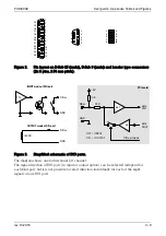
The connector pin layouts are shown in Table 1 through Table 3, the connector pin
assignment is shown in Figure 2 (all in Appendix of this manual).
3.
Installation
PCD-8006
User Guide
rev. 10.2015
I - 3
Содержание PCD-8006
Страница 1: ...Digital I O PCIe card PCD 8006 User Guide ...
Страница 12: ... PCD 8006 User Guide Notes ...
Страница 13: ......
Страница 14: ......


