background image


T3903


Page 6 of 21 

Document Number: DS-000358


Revision: 1.0 


TABLE 5. PDM DIGITAL INPUT/OUTPUT 

T

A

 = 25

°C,


1.8 V


< VDD < 3.3 V 

, unless otherwise noted. 


PARAMETER 

CONDITIONS 

MIN 

TYP 

MAX 

UNITS  NOTES 

MODE SWITCHING 

Sleep Time 

Time from f

CLK

 falling <200 kHz 


ms 


Wake-Up Time 

High Quality  mode, Sleep Mode to f

CLK 

>1.2 

MHz, output within 0.5 dB of final sensitivity, 

power on 


ms 


Wake-Up Time 

Low-Power Mode, Sleep Mode to f

CLK 

>400 

kHz, output within 0.5 dB of final sensitivity, 

power on 


ms 


Switching time 

Between Low-Power and High Quality Mode 


ms 


INPUT


t

CLKIN


Input clock period 

303 


2500 

ns 


Clock Frequency (CLK) 

Sleep Mode 


200 

kHz 


Low-Power Mode 

400 


800 

kHz 


High Quality Mode 

2.0 


3.3 

MHz 


Clock Duty Cycle 

f

CLK

 <3.3 MHz 

45 


55 


t

RISE 

CLK rise time (10% to 90% level) 


25 

ns 

t

FALL 

CLK fall time (90% to 10% level) 


25 

ns 

OUTPUT 

t

1OUTEN


DATA1 (right) driven after falling clock edge 

30 


ns 


t

1OUTDIS


DATA1 (right) disabled after rising clock edge 


18 

ns 


t

2OUTEN


DATA2 (left) driven after rising clock edge 

30 


ns 


t

2OUTDIS


DATA2 (left) disabled after falling clock edge 


18 

ns 


Note 4:

  Guaranteed by design


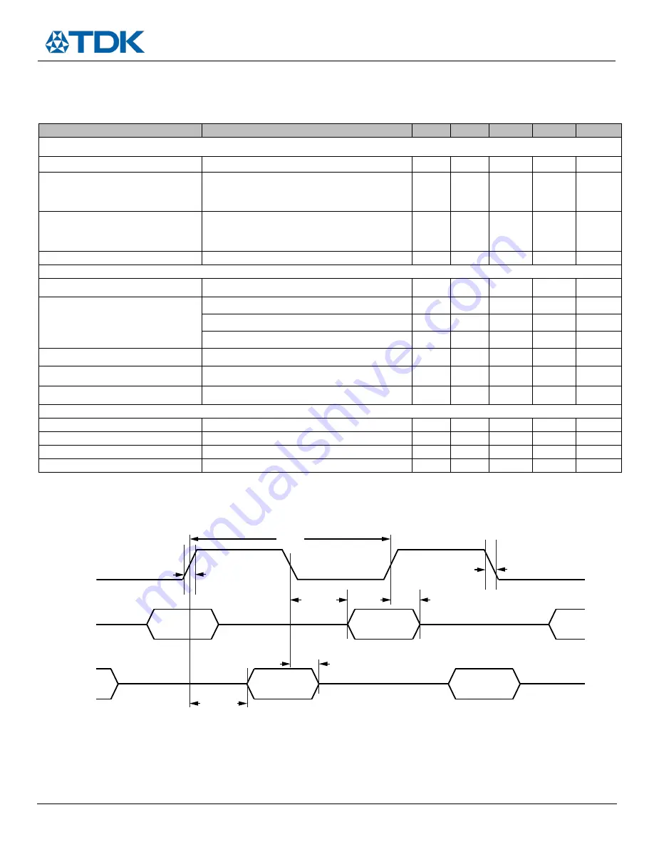
TIMING DIAGRAM 


Figure 1. Pulse Density Modulated Output Timing  

t

CLKIN

CLK

DATA2

DATA1

t

2OUTDIS

t

1OUTDIS

t

2OUTEN

t

1OUTEN

t

RISE

t

FALL

Содержание T3903

Страница 1: ...Sleep The T3903 has high SNR in all operational modes It has 133 dB SPL AOP in High Quality Mode and 120 dB SPL AOP in Low Power mode The T3903 is available in a standard 3 5 2 65 0 98 mm surface moun...

Страница 2: ...Absolute Maximum Ratings 7 Table 6 Absolute Maximum Ratings 7 ESD Caution 7 Soldering Profile 8 Table 7 Recommended Soldering Profile 8 Pin Configurations And Function Descriptions 9 Table 8 Pin Func...

Страница 3: ...T3903 Page 3 of 21 Document Number DS 000358 Revision 1 0 Board Wash 18 Outline Dimensions 19 Ordering Guide 19 Revision History 20 Compliance Declaration Disclaimer 21...

Страница 4: ...MIN TYP MAX UNITS NOTES Sensitivity 1 kHz 94 dB SPL 38 37 36 dB FS 2 Signal to Noise Ratio SNR 20 kHz bandwidth A weighted 66 dBA Equivalent Input Noise EIN 20 kHz bandwidth A weighted 28 dBA SPL Acou...

Страница 5: ...dB SPL 0 15 Power Supply Rejection PSR 217 Hz 100 mV p p square wave superimposed on VDD 1 8 V A weighted 95 dB FS Power Supply Rejection Swept Sine 1 kHz sine wave 99 dB FS Acoustic Overload Point 10...

Страница 6: ...ower and High Quality Mode 7 ms INPUT tCLKIN Input clock period 303 2500 ns Clock Frequency CLK Sleep Mode 200 kHz Low Power Mode 400 800 kHz High Quality Mode 2 0 3 3 MHz Clock Duty Cycle fCLK 3 3 MH...

Страница 7: ...ER RATING Supply Voltage VDD 0 3 V to 3 63 V Digital Pin Input Voltage 0 3 V to VDD 0 3 V or 3 63 V whichever is less Mechanical Shock 10 000 g Vibration Per MIL STD 883 Method 2007 Test Condition B T...

Страница 8: ...1 25 C sec 1 25 C sec Time Maintained Above Liquidous tL 45 sec to 75 sec 50 sec Liquidous Temperature TL 183 C 217 C Peak Temperature TP 215 C 3 C 3 C 260 C 0 C 5 C Time Within 5 C of Actual Peak Tem...

Страница 9: ...t Channel or Right Channel Select DATA 1 right SELECT tied to GND DATA 2 left SELECT tied to VDD In this setting SELECT should be tied to the same voltage source as the VDD pin 3 GND Ground 4 CLK Cloc...

Страница 10: ...10 0 0 0 10 0 20 0 10 100 1000 10000 NORMALIZED AMPLITUDE dB FREQUENCY Hz 0 01 0 10 1 00 10 00 90 100 110 120 130 140 THD N INPUT AMPLITUDE dB SPL High Quality Mode Low Power Mode 120 0 100 0 80 0 60...

Страница 11: ...not enough to discharge the line while the driver is tristated Figure 10 Mono PDM Format See Table 9 for the channel assignments according to the logic level on the SELECT pin The setting on the SELE...

Страница 12: ...an RMS level of 29 dB FS however this is not true because of the definition of the 0 dB FS sine wave Figure 11 1 kHz 0 dB FS Sine Wave There is not a commonly accepted unit of measurement to express t...

Страница 13: ...lly use the 105 dB dynamic range of the output data of the T3903 in a design the digital signal processor DSP or codec circuit following it must be chosen carefully The decimation filter that inputs t...

Страница 14: ...er large capacitive load a digital buffer may be required Only use a signal buffer on the DATA line when one microphone is in use or after the point where two microphones are connected see Figure 14 T...

Страница 15: ...t is in a high impedance state The current consumption in sleep mode is 9 A The microphone wakes up from sleep mode and begins to output data 7 ms after the clock becomes active The wake up time indic...

Страница 16: ...al Output MEMS Microphone Flex Evaluation Board User Guide AN 100 MEMS Microphone Handling and Assembly Guide AN 1003 Recommendations for Mounting and Connecting the TDK Bottom Ported MEMS Microphones...

Страница 17: ...hole in the microphone package with the hole in the PCB The exact degree of the alignment does not affect the microphone performance as long as the holes are not partially or completely blocked Figure...

Страница 18: ...e microphone with a vacuum tool that makes contact with the bottom side of the microphone Do not pull air out of or blow air into the microphone port Do not use excessive force to place the microphone...

Страница 19: ...y LGA_CAV 3 5 mm 2 65 mm 0 98 mm Body Dimensions shown in millimeters Dimension tolerance is 0 15 mm unless otherwise specified Figure 18 Package Marking Specification Top View ORDERING GUIDE PART TEM...

Страница 20: ...T3903 Page 20 of 21 Document Number DS 000358 Revision 1 0 REVISION HISTORY REVISION DATE REVISION DESCRIPTION 1 15 20 0 1 Initial preliminary version 5 5 20 1 0 Initial release...

Страница 21: ...n contained in this document or from the use of products and services detailed therein This includes but is not limited to claims or damages based on the infringement of patents copyrights mask work a...

Отзывы: