S1
S2
S3
T1
T2
T3
U1
U2
U3
V1
V2
V3
W1
W2
W3
S4
T4
U4
V4
W4
REC AUDIO SIGNAL
PB AUDIO (TV/VCR/LINE) SIGNAL
1-10-9
1-10-10
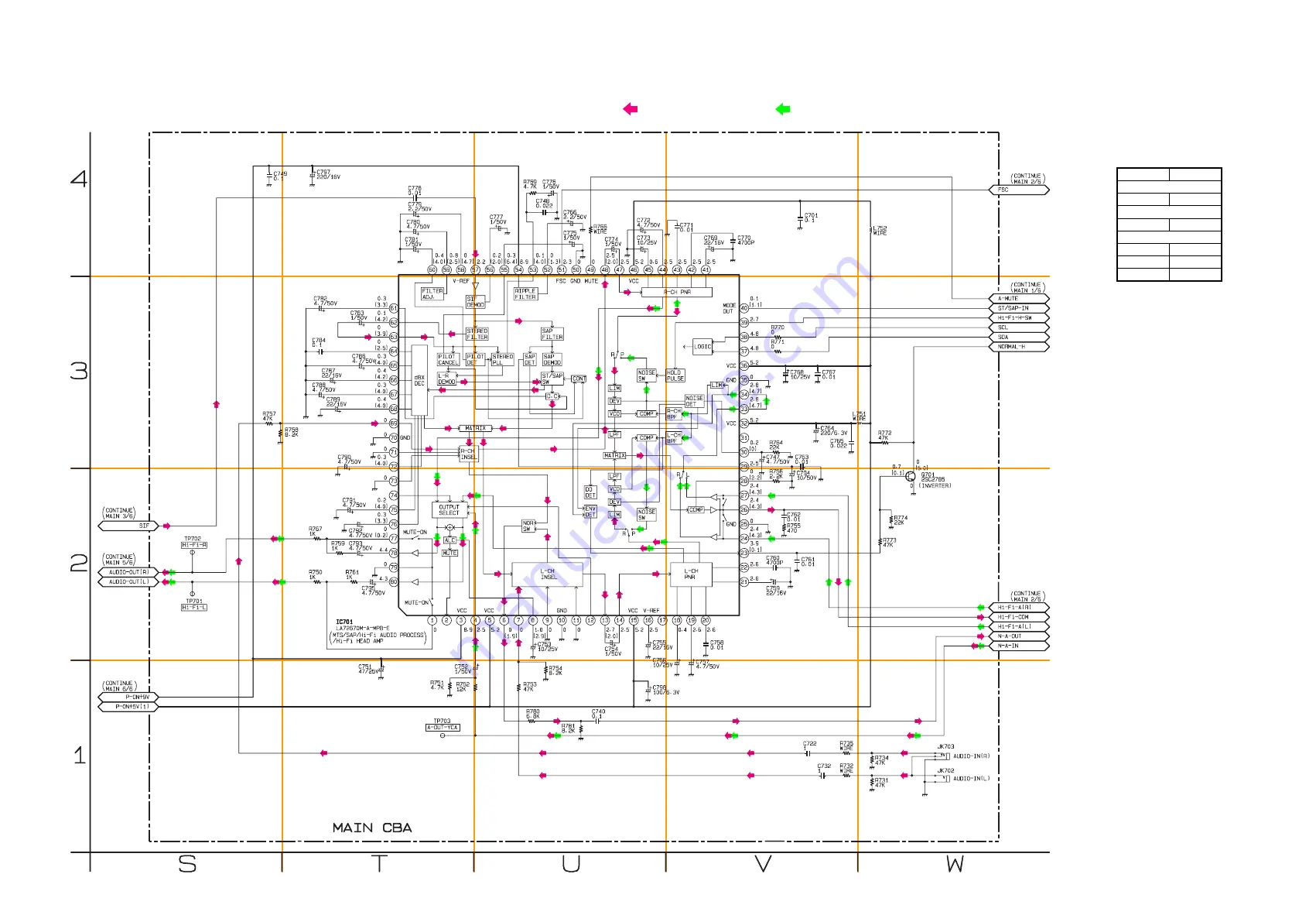
T6001SCM4
Main 4/6 Schematic Diagram < TV/VCR Section >
MAIN 4/6
Ref No.
Position
IC701
T-2
Q701
W-2
TP701
S-2
TP702
S-2
TP703
T-1
IC
TRANSISTOR
TEST POINTS


