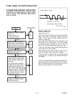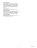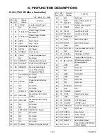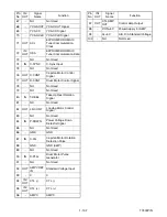
1-8-1
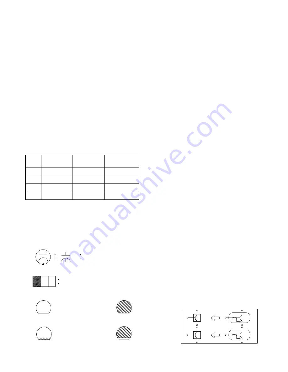
SC_1
(Top View) (Bottom View)
(Bottom View)
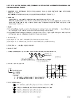
Electrolytic Capacitor
+
Transistor or Digital Transistor
NPN Transistor
PNP Transistor
NPN Digital Transistor
PNP Digital
Transistor
(Top View)
(Top View)
E C B
E C B
Digital Transistor
CBA Symbols
Schematic Diagram Symbols
E C B
(Top View)
(Top View)
E C B
E C B
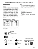
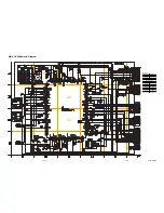
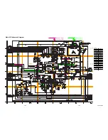
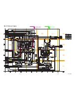
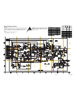
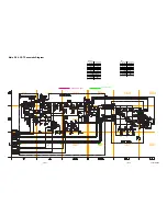
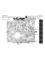
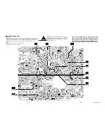
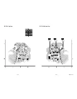
SCHEMATIC DIAGRAMS / CBA’S AND TEST POINTS
Standard Notes
Warning
Many electrical and mechanical parts in this chassis
have special characteristics. These characteristics
often pass unnoticed and the protection afforded by
them cannot necessarily be obtained by using replace-
ment components rated for higher voltage, wattage,
etc. Replacement parts that have these special safety
characteristics are identified in this manual and its
supplements; electrical components having such fea-
tures are identified by the mark "
#
" in the schematic
diagram and the parts list. Before replacing any of
these components, read the parts list in this manual
carefully. The use of substitute replacement parts that
do not have the same safety characteristics as speci-
fied in the parts list may create shock, fire, or other
hazards.
Capacitor Temperature Markings
Capacitors and transistors are represented by the fol-
lowing symbols.
Note:
1. Do not use the part number shown on these draw-
ings for ordering. The correct part number is shown
in the parts list, and may be slightly different or
amended since these drawings were prepared.
2. All resistance values are indicated in ohms (K=10
3
,
M=10
6
).
3. Resistor wattages are 1/4W or 1/6W unless other-
wise specified.
4. All capacitance values are indicated in
µ
F
(P=10
-6
µ
F).
5. All voltages are DC voltages unless otherwise
specified.
Mark
Capacity
change rate
Standard
temperature
Temperature
range
(B)
±
10%
20°C
-25~+85°C
(F)
+30 -80%
20°C
-25~+85°C
(SR)
±
15%
20°C
-25~+85°C
(Z)
+30 -80%
20°C
-10~+70°C
Содержание 6319CE
Страница 17: ...1 5 2 T7500DC ANT 1 REAR CABINET Fig 1 S 1 S 1 S 1 S 2 Fig 2 1 REAR CABINET S 1 S 1 S 2 S 1 S 1...
Страница 18: ...1 5 3 T7500DC Fig 3 S 6 S 5 S 4 S 6 S 6 S 6 S 7 S 3 S 3 2 TRAY CHASSIS 3 DECK UNIT 4 MAIN CBA S 3...
Страница 19: ...1 5 4 T7500DC Fig 4 S 8 S 8 S 8 S 8 5 CRT CRT CBA ANODE CAP...
Страница 56: ...1 14 3 T7500PEX Packing X1 S1 S4 S3 S3 S2 TAPE TAPE X4 X3 X2 X7 S6 S14 FRONT...
Страница 68: ...WF319E 6319CE T7500UA T7502UC 2004 02 26...

