background image

SVS-VISTEK 

Manual SHR series 

Feature-Set    

5.02.2017 

Therefor the signal will not be accepted till it lasts at least a certain time.  

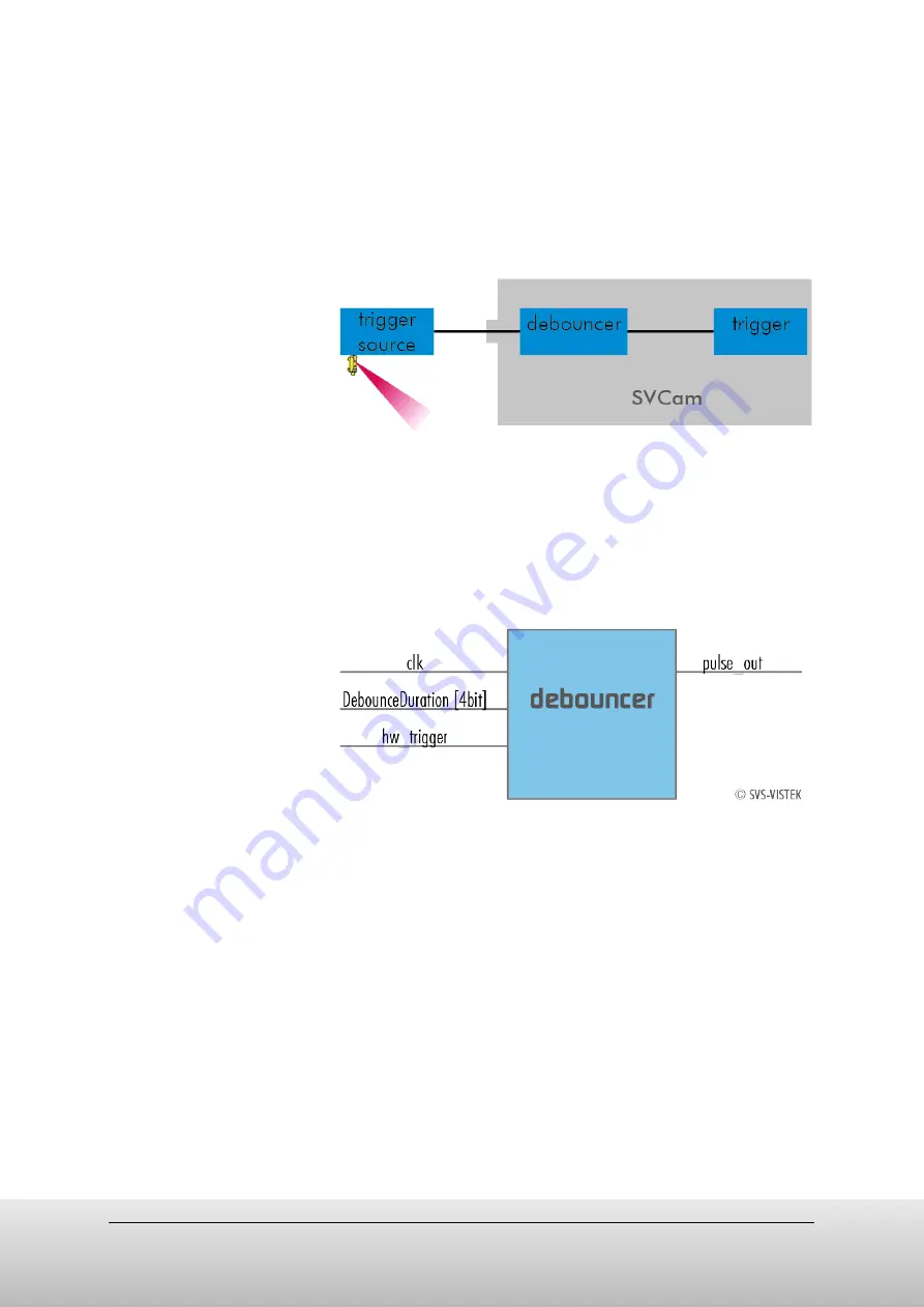
Use the IO Assignment tool to place and enable the debouncer module 
in between the “trigger” (schmitt trigger) and the input source (e.g.: line 
1). 
DebouncDuration register can be set in multiples of 15ns (implement of 

system clock). E.g. 66 666 ≈ 1 ms


Figure 65: block diagram – debouncer in between the trigger source 
and the trigger 


The Debouncer module 


Figure 66: Illustration of the debouncer module 


Содержание Camera Link SHR Series

Страница 1: ...5 02 2017 Manual SHR series shr47051 CL ...

Страница 2: ...site for safe work is compliant with all specified safety and handling instructions Accident prevention guidelines and general safety regulations shoud be applied Illustrations in this Operation Manual are provided for basic understanding and can vary from the actual model of this camera No claims can be derived from the illustrations in this Operation Manual The camera in your possession has been...

Страница 3: ...4 Connectors 16 4 1 Camera Link 16 4 1 1 Connectors Camera Link 16 4 1 2 Pinout Diagram 18 4 1 3 Camera Link timing 19 4 2 Input output connectors 21 5 Dimensions 22 5 1 SHR47051 Camera Link 23 5 2 M72 Mount 26 6 Feature Set 27 6 1 Basic Understanding 27 6 1 1 Basic Understanding of CCD Technology 27 6 1 2 Interline Transfer 28 6 1 3 Global and rolling Shutter 28 6 1 4 Frames per Second 30 6 1 5 A...

Страница 4: ...on 51 6 3 I O Features 52 6 3 1 Assigning I O Lines IOMUX 52 6 3 2 Strobe Control 59 6 3 3 Sequencer 66 6 3 4 PWM 68 6 3 5 Optical Input 69 6 3 6 PLC Logical Operation on Inputs 71 6 3 7 Serial data interfaces 72 6 3 8 Trigger Edge Sensitivity 75 6 3 9 Debouncing Trigger Signals 75 6 3 10 Prescale 77 7 Specifications 78 7 1 shr47051 CL 79 8 Terms of warranty 82 9 Troubleshooting 83 9 1 FAQ 83 9 2 ...

Страница 5: ... or serious injury CAUTION Caution indicates a hazard with a low level of risk which if not avoided will result in death or serious injury Risk of damage PROHIBITION A black graphical symbol inside a red circular band with a red diagonal bar defines a safety sign that indicates that an action shall not be taken or shall be stopped CAUTION A black graphical symbol inside a yellow triangle defines a...

Страница 6: ...ed including interference that may cause undesired operation Note This equipment has been tested and found to comply with the limits for a Class A digital device pursuant to part 15 of the FCC Rules These limits are designed to provide reasonable protection against harmful interference when the equipment is operated in a commercial environment This equipment generates uses and can radiate radio fr...

Страница 7: ...tact us for a recommendation of frame grabbers Some frame grabbers support 1x3 tap configuration With this configuration you might achieve framerates of more than 50 faster than in specs Again contact us for recommended frame grabbers There are different transfer rates with different camera link types Camera Link full 80 bit technology is also known as Camera Link Deca Some models support Power ov...

Страница 8: ...any light to the camera make sure the power supply has enough power not to fail when the camera is putting light ON The integrated sequencer allows multiple exposures with settings to be programmed creating new and cost effective options Logical functions like AND OR are supported Up to 4 x open drain high power OUT Up to 4 x high voltage IN TTL up to 25 Volts Power MOSFET transistors PWM strobe c...

Страница 9: ...en connect power supply When using your own power supply e g 10 25 V DC see also Hirose 12 pin for a detailed pin layout of the power connector For power input specifications refer to specifications 3 3 Camera Link Flashing LED Codes On power up the camera will indicate its current status with a flashing LED on its back The LED will change color and rhythm The meaning of the blinking codes transla...

Страница 10: ...on the type of camera you bought several software packages apply 3 4 1 Installation of ConvCam5 Your SVCam combined software installer including SVConvCam a controller app for SVCam Camera Link cameras TL_Driver GenICam drivers and transport layer DDLs 1st Expand ZIP Extract the zip archive to your local hard drive 2st Install Run the executable file 1 Click Install Click Next CAUTION Make sure yo...

Страница 11: ...017 Read and accept terms of License Agreement Choose Options 2 and Location to install Click Finish 1 x64 for 64 bit operating systems x86 for 32 bit operating systems 2 It is recommended to install all applications included to the installation package ...

Страница 12: ... N N E E D E D B Y Y O U R F R A M E G R A B B E R Tap configuration Trigger mode Pixel width and height 3 4 3 ConvCam5 Set values as needed 3 4 4 Viewer Software The final image will be shown or processed by your own valued software package After camera configuration an image will be directed to the software connected to your frame grabber E g Multicam by Euresys While using a Euresys frame grabb...

Страница 13: ...Click next In the list of camera vendors choose SVS VISTEK and the camera you want to view Select frame grabber and connector For Topology values refer to the Euresys documentation At first stay with Mono for topology Choose your connector configuration click Finish Now an image should appear according to your setup configurations made with ConvCam ...

Страница 14: ...SVS VISTEK Manual SHR series Getting Started 5 02 2017 For further information on Euresys Multicam Studio refer to the documentation from Euresys ...

Страница 15: ...SVS VISTEK Manual SHR series Getting Started 5 02 2017 3 5 Driver Circuit Schematics Figure 3 basic Illustration of driver circuit ...

Страница 16: ...k a frame grabber is needed Frame grabbers can be purchased at SVS VISTEK too 4 1 1 Connectors Camera Link Specification Type 26 Pin connector MDR female Mating Connector 3M Part Nr connector 10126 6000EL Part Nr hood 10326 A200 00 Operating Mode Camera Link with RS 232 communication ...

Страница 17: ... 10 CC2 FG to Camera Prin not used 11 CC3 FG to Camera External Camera Clock 12 CC4 FG to Camera nc 13 GND Shield 3 power return 14 GND Shield 2 power return 15 X0 Camera to FG Data 16 X1 Camera to FG Data 17 X2 Camera to FG Data 18 Xclk Camera to FG Transmitter Clock 19 X3 Camera to FG Data 20 SerTC FG to Camera Camera Control RS232 21 SerTFG Camera to FG Camera Control RS232 22 CC1 FG to Camera ...

Страница 18: ...SVS VISTEK Manual SHR series Connectors 5 02 2017 4 1 2 Pinout Diagram Figure 5 Illustration of Camera Link pin out ...

Страница 19: ...with no valid data The Duration of None Valid Data between two lines tnvd is three time the Camera Link clock clk Delay before every first line is 2 times clk 𝑡𝐿𝐿𝐿 𝑝𝑝ℎ 𝐶𝐶_𝑔𝑔𝑔𝑔𝑔𝑔𝑔𝑔_𝑋 1 𝐶𝐶_𝑐𝑐𝑐𝑐𝑐 CL_clock 85 MHz FVAL tFv d Frames are not sent permanently Between two frames will be a gap even at highest frame rates Minimum duration between two valid frame signals is the duration of one line 𝑡𝐹𝐹𝐹 2 1 𝐶...

Страница 20: ...ent at once 1 85MHz CL_clock 960 1 85e6 s 11 29 µs tnvd 3 1 85MHz time between two valid line data packages 3 85e6 s 35 3 ns tFvd 2 x 1 85MHz delay before first line tLVd tnvd 1200 lines count 2 85e6 s 11 29 µs 35 3 ns 1200 23 5 ns 11 29 µs 35 3 ns 1200 2 960 3 1200 s 85e6 13 6 ms Camera Link architecture exo174 CL 1X2_1Y count 2 pixelh 1920 pixelv 1200 CL_clock 85 MHz Figure 8 example calculation...

Страница 21: ...ion refer to SVCam Sensor Actor manual with Murr and Phoenix breakout boxes To be found separate within the USP manuals Hirose 12Pin For detailed information about switching lights from inside the camera refer to strobe control Specification Type HR10A 10R 12S Mating Connector HR10A 10R 12P Figure 9 Illustration of Hirose 12 Pin pin out HR10A 10R 12PB ...

Страница 22: ...SVS VISTEK Dimensions Input output connectors 22 5 Dimensions All length units in mm CAD step files available on DVD or SVS VISTEK com ...

Страница 23: ...mensions 5 02 2017 5 1 SHR47051 Camera Link front side Left ATTENTION The blue red metal bar is the heatsink of the sensor itself Do not attach anything here Attaching devices to the colored metal bar will deadjust destroy the sensor ...

Страница 24: ...SVS VISTEK Manual SHR series Dimensions 5 02 2017 Top Bottom ...

Страница 25: ...SVS VISTEK Manual SHR series Dimensions 5 02 2017 Back Cross Section ...

Страница 26: ...ions 5 02 2017 5 2 M72 Mount Diameter 72 mm Mechanical sensor flange distance 19 90mm Including the cover glas to the calculation of the distance the optical sensor flange distance shrinks to 19 57 mm Figure 10 Illustration of M72 mount ...

Страница 27: ...nts a single line in the resulting image When light falls onto the sensor elements photons are converted into electrons creating a proportional light input signal Figure 11 Illustration Cross section of a CCD sensor from Sony Charge is an integration of time and light intensity on the element Like this the image gets brighter the longer the CCD cell is exposed to light The sensor converts light in...

Страница 28: ...the horizontal register and read out the vertical registers can accept the next image Figure 12 Illustration of interline transfer with columns and rows 6 1 3 Global and rolling Shutter CCD and CMOS cameras are consisting of pixels All pixel are exposed to light and then read out to camera electronics There is a difference of reading out the sensor between global and rolling shutter Especially fla...

Страница 29: ...ime in the image A global shutter image is a snapshot of the whole scene Figure 13 motion blur with global shutter and moving objects Figure 14 rolling shutter with moving objects geometric distortion Figure 15 interlaced effect Using flash with global shutter is simpel just make sure your flash is on while shutter is open ...

Страница 30: ...5 4 s 1 1s 2 500ms 20 50 ms 24 41 6 ms Cinema 25 40 ms PAL progressive 29 97 33 366700033 ms NTSC 30 33 33 ms NTSC 50 20 ms PAL interlaced 75 13 33 ms 100 10 ms Virtually any value within the specification can be chosen Maximum frame rate depends on Pixel clock Image size Tap structure Data transport limitation Processing time 6 1 5 Acquisition and Processing Time The whole period of tome a pictur...

Страница 31: ... the gain The first priority is to adjust the exposure time and if the exposure time range is not sufficient gain adjustment is applied It is possibility to pre define the range min max values of exposure time and of gain The condition to use this function is to set a targeted averaged brightness of the camera image The algorithm computes a gain and exposure for each image to reach this target bri...

Страница 32: ... 256 values per pixel 12 bits to 212 4096 values per pixel 16 bit to 216 65536 values per pixel Every additional bit doubles the number for quantification SVCam output is 8 12 or 16 bit depending on your camera model and the way you read the values from the camera Be aware that increasing the bit format from 8 to 12 bit also increases the total amount of data According to the interface framerates ...

Страница 33: ...SVS VISTEK Manual SHR series Feature Set 5 02 2017 Figure 20 Figure of original picture black white Figure 21 Figure of quantification with 6 shades of gray reduced colour depth ...

Страница 34: ...nts The performance of the image depends on the software used NOTICE It is recommended to use a IR cut filter for color applications White Balance The human eye adapts to the definition of white depending on the lighting conditions The human brain will define a surface as white e g a sheet of paper even when it is illuminated with a bluish light White balance of a camera does the same It defines w...

Страница 35: ...rence between the active and the effective resolution of almost every sensor Some pixels towards the borders of the sensor will be used only to calibrate the sensor values These pixels are totally darkened The amount of dark current in these areas is used to adjust the offset Figure 24 Illustration of active and effective sensor pixels ...

Страница 36: ...f dark noise cut off by the offset Most noise is proportional to temperature To spare you regulating the offset every time the temperature changes A precedent offset is set by the camera itself It references certain pixels that never were exposed to light as black refer to resolution active and effective So the offset will be set dynamically and conditioned to external influences The offset can be...

Страница 37: ...g to Photography adding gain corresponds to increasing ISO add 6 dB double ISO value 6 dB 400 ISO 12 dB 800 ISO 18 dB 1600 ISO 24 dB 3200 ISO Figure 26 Table of dB and corresponding ISO NOTICE Gain also amplifies the sensor s noise Therefore gain should be last choice for increasing image brightness Modifying gain will not change the camera s dynamic range Figure 27 noise caused by increasing gain...

Страница 38: ...ages can be mirrored horizontally or vertically Image flip is done inside the memory of the camera therefore not increasing the CPU load of the PC Figure 28 Figure of original image Figure 29 Figure of image horizontally flipped Figure 30 Figure of image vertically flipped ...

Страница 39: ...rge from neighboring pixels directly on the chip before readout Binning is only used with monochrome CCD Sensors For reducing resolution on color sensors refer to decimation Vertical Binning Accumulates vertical pixels Figure 31 Illustration of vertical binning Horizontal Binning Accumulates horizontal pixels Figure 32 Illustration of horizontal binning 2 2 Binning A combination of horizontal and ...

Страница 40: ...ducing data rate by reducing the region you are interested in Figure 34 Horizontal decimation Figure 35 Vertical decimation Decimation on Color Sensors The Bayer pattern color information is preserved with 1 3 horizontal and vertical resolution The frame readout speed increases approx by factor 2 5 Figure 36 Illustration of decimation on color sensors 6 1 16 Burst Mode The hardware interface GigE ...

Страница 41: ...t process of the camera on USB cameras the maximum sensor speed is limited to the maximum interface speed This means the maximum trigger frequency cannot be higher than camera freerun frequency The image buffer will protect against breaking datarates of the USB line though Usage of Burst Mode Burst Mode has 2 main purposes If transfer speed breaks down e g Ethernet transfer rate due to high networ...

Страница 42: ...n be sent in parallel The tap geometry is describing how many taps are read and how they are transmitted through the Camera Link interface 6 2 2 Tap Structure Your camera may be equipped with a two four or even higher taped sensor Tap configuration For information according to your sensor refer to specifications Figure 38 Illustrations of the nomenclature used in specifications Single Tap Camera T...

Страница 43: ...of 2 taps In a dual tap CCDs CCD with two outputs the readout of pixel charge takes place in a serial parallel sequence Each line is divided in half and the pixels of both halves are read out simultaneously line by line For a given pixel clock frequency only half the time is required to read out the entire array resulting in twice the framerate Figure 42 Illustration of 2 taps Quad Tap Figure 43 F...

Страница 44: ...nalog signal coming from the CCD The fact that the separate analog output channels not being perfectly linear and the separate output amplifiers having physically different slopes leads to the necessity to sometimes manually or automatically adjust the gain levels of each channel independently to obtain a homogenous image Automatic Tap Balancing Automatic Tap Balancing analyses a narrow strip at t...

Страница 45: ...of time time settings can only be made in multiples of 15 ns 𝑡 1 66 6 𝑀𝑀𝑀 1 66 666 666 6 1 𝑠 15 10 9 𝑠 15 𝑛𝑛 NOTICE Use multiples of 15 ns to write durations into camera memory 6 2 5 Temperature Sensor A temperature sensor is installed on the mainboard of the camera To avoid overheating the temperature is constantly monitored and read Besides software monitoring the camera indicates high temperatu...

Страница 46: ...d Mode pulse width External trigger and pulse width controlled exposure time In this mode the camera is waiting for an external trigger which starts integration and readout Exposure time can be varied using the length of the trigger pulse rising edge starts integration time falling edge terminates the integration time and starts frame read out This mode is useful in applications where the light le...

Страница 47: ...igger the camera will initiate the exposure The software provided by SVS Vistek allows the user to set exposure time e g from 60 μs 60 Sec camera type dependent Exposure time of the next image can overlap with the frame readout of the current image trigger pulse occurs when FVAL is high When this happens the start of exposure time is synchronized to the negative edge of the LVAL signal see figure ...

Страница 48: ...al SHR series Feature Set 5 02 2017 Software Trigger Trigger can also be initiated by software serial interface NOTICE Software trigger can be influenced by jitter Avoid Software trigger at time sensitive applications ...

Страница 49: ...igure 46 Illustration of AOI limitation on a CCD sensor Selecting an AOI will reduce the number of horizontal lines being read This will reduce the amount of data to be transferred thus increasing the maximum speed in term of frames per second With CCD sensors setting an AOI on the left or right side does not affect the frame rate as lines must be read out completely ...

Страница 50: ...hallenging conditions or high temperature environments additional defect pixels can may appear These can be corrected A factory created defect map SVS map defying known defects is stored in the camera A custom defect map can be created by the user A simple txt file with coordinates has to be created The user must locate the pixel defects manually The txt file can be uploaded into the camera Beware...

Страница 51: ... side 10 or 12 bit loss of dyn range In the camera analog Change gain offset locally on sensor to get optimum shading correction with only small changes in dynamic range Performing builtin shading correction In order to perform a correction for an image with non uniform image a reference white image is captured This will allow creating correction values to adjust the pixels by individual gain sett...

Страница 52: ...ction disabled Save it on disk Use std bmp files here if possible with more than 8 bit With the shading tool SVCamCC5_Shading load this reference image Select the Map position out of positions 012 By uploading the generated shading map will be written to the camera If you want to have it persistent press SAVE TO EEPROM Verify the result by selecting a map and press SELECT MAP You can remove any sh...

Страница 53: ...u connect the camera with a non SVS Vistek GigEVision client you might not see the clearnames of the lines but only line numbers In this case use this list of line names LineSelector translation Line0 Output0 Line1 Output1 Line2 Output2 Line3 Output3 Line3 Output4 Line5 Uart In Line6 Trigger Line7 Sequencer Line8 Debouncer Line9 Prescaler Line10 Input0 Line11 Input1 Line12 Input2 Line13 Input3 Lin...

Страница 54: ...ally wiring Also the IOMUX can be illustrated as a three dimensional dice Long address spaces indicate which signals are routed to witch module within the camera Figure 50 illustration of the backside view of the camera mudules The side of the switch matrix connections will be made withn a 1 instead of a 0 ...

Страница 55: ...SVS VISTEK Manual SHR series Feature Set 5 02 2017 Figure 51 illustration of frontside view to the camera modules Lines with open end indicate physical in and outputs ...

Страница 56: ...odule iomux_sequenzer_0 10 expose input 11 readout input 12 r_sequenzer_pulse_a output from module iomux_sequenzer_0 pulse 13 rr_pwm_out_c output from module iomux_sequenzer_0 14 rr_pwm_out_d output from module iomux_sequenzer_0 15 r_sequenzer_active output from module iomux_sequenzer_0 16 r_debouncer output from module iomux_dfilter_0 17 r_prescaler output from module iomux_prescaler_0 18 r_seque...

Страница 57: ...nzer_0 8 debounce input input to module iomux_dfilter_0 9 prescale input input to module iomux_prescaler_0 10 logic inputa input to module iomux_logic_0 11 logic inputb input to module iomux_logic_0 12 mft_txd output 13 pulseloop hw_trigger input to module iomux_pulseloop_0 14 pulseloop hw_trigger input to module iomux_pulseloop_1 15 pulseloop hw_trigger input to module iomux_pulseloop_2 16 pulsel...

Страница 58: ...hat the camera is exposing the sensor connect line 17 to 14 signal from pulse loop module 1 appears on line 7 connect line 7 to 1 output 1 Turn of a light that was ON during the time between two pictures connect line 17 to 15 invert signal from pulse loop module 2 it appears on line 20 connect line 20 to 2 output 2 Inverter Set to 1 Inverter and set to 1 is part of every input and every output of ...

Страница 59: ...ferent channels that can be used simultaneously or independent from each other According to the I O specification of your camera two or four channels can be used as open drain Refer to specifications 4 IO high voltage drain Figure 52 Illustration of four LEDs switched internal by the camera For detailed connector pin out refer to Connectors For further information using the breakout box and simpli...

Страница 60: ...SVS VISTEK Manual SHR series Feature Set 5 02 2017 Figure 53 Illustration of conventional schematic electric circuit Figure 3 4IO simplifies light control ...

Страница 61: ...SVS VISTEK Manual SHR series Feature Set 5 02 2017 Figure 4 Illustration of schematic wiring with 4IO model using the break out box matrix ...

Страница 62: ... HW trigger Pulse output starting on low or high level Pre and post duration time Number of loops E X A M P L E A P P L I C A T I O N S Initiated by an external trigger the camera drives an LED illumination directly from the open drain output and initiates the camera exposure after a pre defined delay Figure 54 pulseloop for strobe and exposure C A M E R A C A S C A D E Three cameras are triggered...

Страница 63: ...ee spec of LED 250 mA Voltage Supply 24 V Voltage drop at Resistor 24 V 11 V 13 V Pull up Resistor R 𝟏𝟏 𝑽 𝟐𝟐𝟐 𝒎𝒎 52 Ω Total Power 𝑷 𝑼 𝑰 6 W Power at LEDs 𝟏𝟏 𝑽 𝟐𝟐𝟐 𝒎𝒎 2 75 W Power Loss at Resistor 𝟏𝟏 𝑽 𝟐𝟐𝟐 𝒎𝒎 3 25 W USE RIGHT DIMENSION OF RESISTOR Protect your display from damage by selecting the appropriate resistor dimension The PWM output will put full operational voltage to the LED display ...

Страница 64: ...eans the off time is 850 mSec The sum of time on and time off is 1000 mSec 1 Sec NOTICE The shorter the time on the higher current can be used the longer LEDs will work Strobe Timing 6 3 2 1 1 Exposure Delay A value representing the time between the logical positive edge of trigger pulse and start of integration time Unit is 1μs Default is 0μs 6 3 2 1 2 Strobe Polarity Positive or negative polarit...

Страница 65: ...SVS VISTEK Manual SHR series Feature Set 5 02 2017 Strobe Control Example Setup Figure 56 Illustration of an application using the 4IO ...

Страница 66: ...terval Exposure Start µs Exposure delay after Interval start Exposure Stop µs Exposure Stop related to Interval Start Strobe Start µs Strobe delay after Interval start Strobe Stop µs Strobe Stop related to Interval Start PWM Frequency T Basic duty cycle 1 Hz for PWM PWM Line 1 Demodulation Result PWM Line 2 Demodulation Result PWM Line 3 Demodulation Result PWM Line 4 Demodulation Result Values ca...

Страница 67: ...e Start 220 000 µs 875 000 µs 190 000 µs Exposure Stop 700 000 µs 125 000 µs 720 000 µs Strobe Start 110 000 µs 125 000 µs 350 000 µs Strobe Stop 875 000 µs 875 000 µs 875 000 µs PWM Frequency 4 Hz 4 Hz 4 Hz PWM Line 0 100 0 80 PWM Line 1 20 50 0 PWM Line 2 0 100 30 PWM Line 3 Trigger set to negative slope Use higher frequencies Figure 57 illustration of three sequencer intervals ...

Страница 68: ...mance at a certain voltage range such as diodes or LEDs Diode characteristic Since LEDs have a bounded workspace the PWM ensures a variable intensity of illumination at a constant voltage on the diodes In addition the lifetime of a diode increases The internal resistance is ideal in this area The diode gets time to cool down when operated with a PWM in its workspace Implementation of PWM Modulatio...

Страница 69: ...ty Figure 59 50 intensity Figure 60 75 intensity The integrals over both periods 𝑇𝐴 and 𝑇𝐴 are equal 𝐀 𝑡𝐴2 𝑡𝐴1 𝐁 𝑡𝐵2 𝑡𝐵1 An equal amount of Photons will be emitted The intensity of light is the same 𝑡𝐴2 𝑡𝐴1 𝑡𝐵2 𝑡𝐵1 The periods 𝑇𝐴 and 𝑇𝐵 are equal in length T H E P W M M O D U L E 6 3 5 Optical Input An optical input is designed for galvanic separation of camera and triggering device Noise transien...

Страница 70: ...t it is slower in terms of signal transmission than a direct electrical connection An optical input needs some current for operation The SVS Vistek optical input is specified to 5 24V 8mA The opto coupler galvanically divides electrical circuits by emitting light on one side and interpreting light in the other There is no direct electric interaction between both electrical circuits Figure 5 Optica...

Страница 71: ...ct 2 signals on the logic input The result can be connected to a camera trigger signal or it may be source for the next logical operation with another input It is possible to connect it to an OUT line as well AND Both trigger inputs have to be true A B Y A B 0 0 0 0 1 0 1 0 0 1 1 1 NAND The NEGATIVE AND is true only if its inputs are false Invert the output of the AND module A B Y A NAND B 0 0 1 0...

Страница 72: ...lts in a high or a low level pulse_out Invert both trigger inputs By inverting the resulting pulse_out you will get the NOR I pulse A B Y A B NOR Y A B NOR i 0 0 1 0 0 1 0 1 1 0 0 1 1 1 0 1 6 3 7 Serial data interfaces ANSI EIA TIA 232 F RS 232 and RS 422 from EIA read as Radio Sector or commonly as Recommended Standard are technical standards to specify electrical characteristics of digital signa...

Страница 73: ...Signal voltage values are low 3 15 V high 3 15 V With restrictions refer to Table serial interface parameter above Data transportis asynchronous Synchronization is implemented by fist and last bit of a package Therefore the last bit can be longer e g 1 5 or 2 times the bit duration Datarate bits per second must be defined before transmission Serial interface Parameter RS 232 RS 422 Maximum open ci...

Страница 74: ... stop bits is implemented by the UART Universal Asynchronous Receiver Transmitter Figure 61 UART encoding of a data stream RS 422 RS 422 is a differential low voltage communication standard Figure 62 LVDS signal no return to zero volt Refer to specifications to see if RS 422 is implemented in your camera ...

Страница 75: ... Instead of triggering to a certain value Schmitt trigger provides a threshold Figure 63 illlustration of schmitt trigger noise suspension high to low I low to high 6 3 9 Debouncing Trigger Signals Bounces or glitches caused by a switch can be avoided by software within the SVCam Figure 64 bounces or glitches caused by a switch during 300 µs ...

Страница 76: ...to place and enable the debouncer module in between the trigger schmitt trigger and the input source e g line 1 DebouncDuration register can be set in multiples of 15ns implement of system clock E g 66 666 1 ms Figure 65 block diagram debouncer in between the trigger source and the trigger The Debouncer module Figure 66 Illustration of the debouncer module ...

Страница 77: ... bit word resulting in 16 unique settings Reducing count of interpreted trigger signal Use the prescaler to ignore a certain count of trigger signals Divide the amount of trigger signals by setting a divisor Maximum value for prescale divisor is 16 4 bit Figure 67 illustration of prescale values The prescale module Figure 68 Illustration of the prescale module ...

Страница 78: ...ations I O Features 78 7 Specifications All specifications can be viewed as well on our website www svs vistek com We are proud to have ongoing development on our cameras so specs might change and new features being added ...

Страница 79: ... 5x5 5 µm 5 5x5 5 µm optic sensor w x h 48 7x29 mm 48 7x29 mm exposure time 28 µs 1s 28 µs 1s max gain 18 dB 18 dB dynamic range 62 dB 62 dB S N Ratio 42 6 42 6 frame buffer 256 MB 256 MB CL_geometry 1x2 1y 1x2 2ye 1x2 1y 1x2 2ye frequency select camera pixel clock 40 MHz 40 MHz exp time adjustment manual auto external manual auto external px format 8 12 16 x x x x packed readout max binning h v 2...

Страница 80: ...in out 1 1 RS 232 in out 1 1 1 1 RS 422 in out power supply 10 25 V 10 25 V lens mount M72x0 75 M72x0 75 dynamic lens control size w h d 1 80x80x69 1 mm 80x80x69 1 mm weight 560 g 560 g protection class IP30 IP30 power consumption 15 0 W 15 0 W ambient temperature 10 45 C 10 45 C rel humidity non condensing 0 0 0 0 status production production 1 please refer to model drawings SVS VISTEK May 2 2017...

Страница 81: ...S VISTEK Manual SHR series Specifications 5 02 2017 Spectral Sensitivity Characteristics Figure 6 Spectral Sensitivity Characteristics KAI 47051 F Figure 7 Spectral Sensitivity Characteristics KAI 47051 A ...

Страница 82: ...authorization is issued Seller will inform Buyer of related repair and or replacement costs and request authorization before incurring such costs Buyer shall identify all returned material with Sellers invoice number under which material has been received If more than one invoice applies material has to be clearly segregated and identified by applicable invoice numbers Adjustment is contingent upo...

Страница 83: ...s are not present or don t have the proper quality the camera cannot read out any frame Mode 1 and 2 Beware of spikes on the signal Image is present but distorted Check the camera configuration file of your frame grabber Check number of front and back porch pixel Wrong numbers in configuration file can cause sync problems Check if your frame grabber can work with the data rate of the camera Image ...

Страница 84: ...a Specific Problem Solution Operating in CameraLink Medium lower half of image is black After Load Default User Sets the camera will be set to 8 tap mode 2X_1Y Set the camera to your required tap mode 2T8 tap geo 2X2YE in CL Base 4T8 or 4T12 geo 2X_2YE in CL Medium ...

Страница 85: ...stem E g Win 7 XP Which Camera are you using Type e g svs3625MTHCPC Serial Number Which Accessories are you using Power Supply Cable Lens Type and Focal Length Firmware No of Version Operation Mode Please send a screenshot of ConvCam screen or log file In case of EURESYS Grabber Brand and Type Driver Version If Patch please specify Camera file used Short Description of Problem E g missing lines no...

Страница 86: ...SVS VISTEK Manual SHR series Troubleshooting 5 02 2017 Space for further descriptions screenshots and log files ...

Страница 87: ...t when the enclosure is at an angle of 15 either side of the vertical 2 Protected against water droplets Droplets falling vertically must not have any harmful effect with enclosure at an angle of 15 either side of the vertical 3 Protected against spray water Water sprayed at any angle of up to 60 either side of the vertical must not have any harmful effect 4 Protected against water splashes Water ...

Страница 88: ... the National Semiconductor interface Channel link It was designed for the purpose of standardizing scientific and industrial video products including cameras cables and frame grabbers Charge Coupled Device Commonly used technology used for camera sensors used to detect quantify light i e for capturing images in an electronic manner CCDs were first introduced in the early 70ies Complementary Metal...

Страница 89: ...ines above and below the desired area Typically applied to CCD sensors In most CMOS image sensors an AOI area of interest or ROI region of interest can be defined by selecting the area to be read This leads to increased frame rate The base clock beat that operates the sensor chip is It is typically also the clock with which pixels are presented at the output node of the image sensor A camera RAW i...

Страница 90: ...standard USB 3 0 interface and uses USB 3 0 ports Components from different manufacturers will easily communicate with each other Cameras for industrial use usually provide a set of different trigger modes with which they can be operated The most common trigger modes are 1 Programmable shutter trigger mode Each image is captured with a pre defined shutter time 2 Pulse Width Control trigger The ima...

Страница 91: ...etric distortion 29 Figure 15 interlaced effect 29 Figure 1 illustration of rising amount of values gray scales by increasing the bit format 32 Figure 3 Simplified illustration of a quantification graph 32 Figure 18 illustration of shade difference in 8 bit format 32 As shown in figure 19 differences in shades of gray are hardly visable on screen or in print 32 Figure 20 Figure of original picture...

Страница 92: ...l be made withn a 1 instead of a 0 54 Figure 5 illustration of frontside view to the camera modules 55 Figure 52 Illustration of four LEDs switched internal by the camera 59 Figure 53 Illustration of conventional schematic electric circuit 60 Figure 54 pulseloop for strobe and exposure 62 Figure 55 pulseloop activating three cameras 62 Figure 9 Illustration of an application using the 4IO 65 Figur...

Страница 93: ...Flashing LED Codes 9 Camera Link 16 Camera Specific 84 CCD 27 36 39 44 49 Clock 45 Color 34 40 Connecting the camera 12 Connectors 16 Connectors Camera Link 16 Contents of Camera Set 9 Continuously Tap Balancing 44 ConvCam 85 ConvCam5 10 12 Correct shading with Shading Tool 52 Correction 50 Cross Section 25 Cycle duration 68 dark noise 36 dB 37 debouncer 52 76 Debouncing 75 Debouncing Trigger Sign...

Страница 94: ...am5 10 Interline Transfer 28 interval 66 Inverter 58 Inverter Set to 1 58 IO Assignment 75 IP protection classes 87 IR cut filter 34 ISO 37 Kelvin 34 LED 45 LED Codes 9 LEDs 68 LEDs in Flash Mode 64 Legal Information 6 Light sources 34 Limitation 31 log file 85 Luminance 31 LVAL 46 LVAL tLvd 19 LVDS 74 M72 Mount 26 Manual Tap Balancing 44 MHz 45 Modulation frequency 68 NAND 71 no return to zero vo...

Страница 95: ...Standard Tap Geometries 42 Strobe 52 Strobe Control 59 Strobe Control Example Setup 65 Strobe Delay 64 Strobe Duration 64 Strobe Polarity 64 Strobe Timing 64 Support Request Form 85 Support Request Form Check List 85 System Clock Frequency 45 Tap 44 Tap Balancing 44 Tap Balancing once 44 Tap configuration 42 Tap Reconstruction on Camera Link 44 Tap Structure 42 temperature 36 45 Temperature Sensor...

Отзывы: