


62
X10SRM-F/-TF User Manual
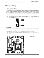
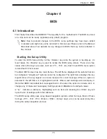
IPMI_LAN
USB0/1
LAN1
LAN2
USB6/7
(3.0)
JPL1
JSTBY1
JPG1
JTPM1
COM2
COM1
FAN4
JF1
JPH1
JPV1
JPW1
FAN1
JPI2C1
FAN2
FAN3
FANA
JPUSB1
USB10 (3.0
)
USB8/9 (3.0
)
USB4/5
I-SGPIO2
I-SGPIO1
JS1
JL1
USB2/3
JP3
JWD1
JPME2
JI2C2
JI2C1
JPB1
JBT1
BT1
JMD1
JNVI2C
1
JIPMB1
LEDBMC
LEDPWR
LE8
LE1
JUIDB1
VGA
JPCIE4
JPCIE5
JPCIE6
CPU1 SLOT6 PCI-E 3.0 X1
6
CPU1 SLOT5 PCI-E 3.0 X8
CPU1 SLOT4 PCI-E 3.0 X8
FAN5
I-SA
TA
3
SP1
I-SA
TA
2
I-S
AT
A1
I-SA
TA
0
I-SA
TA
5
I-SATA4
JSD2
JSD1
JPH2
DIMMA
1
DIMMB
1
DIMMD
1
DIMMC
1
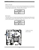
CLOSE 1st
OPEN 1st
MAC
CO
DE
BAR
CO
DE
BAR
CO
DE
CPU
INTEL PCH
LAN
CONTROLLER
X10SRM-F/-TF
REV:1.01
Designed in the USA
SRW5
SRW4
SRW3
JVRM
2
JVRM
1
JOH1
JD1
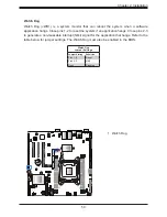
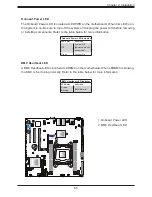
1. M.2 I
2
C Enable/Disable
2. JVRM1/JVRM2
M.2 Slots I
2
C Enable/Disable
Jumper JP3 is used to enable or disable I
2
C for the M.2 connector located at JMD1. Refer
to the table below for jumper settings.
1
2
I
2
C Bus for VRM
Jumpers JVRM1 and JVRM2 allow the BMC or the PCH to access the CPU and memory
voltage regulator modules (VRM) controllers. Refer to the table below for jumper settings.
VRM
Pin Definitions
Pin#
Definition
1-2
BMC (Default)
2-3
PCH
M.2 Slots I
2
C
Pin Definitions
Pin#
Definition
1-2
Normal
2-3
Disable
Содержание X10SRM-F
Страница 1: ...USER MANUAL Revision 1 0a X10SRM F TF...
Страница 8: ...8 X10SRM F TF User Manual Notes...
Страница 11: ...11 Chapter 1 Introduction Figure 1 2 X10SRM TF Motherboard Image...
Страница 66: ...66 X10SRM F TF User Manual Notes...
Страница 116: ...X10SRM F TF User Manual 116 Notes...
Страница 122: ...X10SRM F TF User Manual 122 Notes...