17
Chapter 1: Introduction
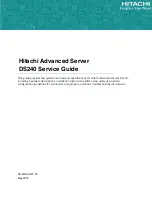
Figure 1-5. Intel PCH C621 Chipset: System Block Diagram
Notes:
•
This is a general block diagram and may not exactly represent the features on your moth-
erboard. See the System Specifications appendix for the actual specifications of your
motherboard.
•
Support for 2933 MHz memory is dependent on the processor SKU.
#0
#1
#1
#2
BMC Boot Flash
RJ45
C621
SSATA #0-1
SSATA #4-5
USB3.0 #1-2
USB3.0 #1-2
X11DSC
CPU1-C1 CPU1-B1 CPU1-A1 CPU1-A2
DDR
4
2666/2933
DDR
4
2666/2933
DDR
4
2666/2933
DDR
4
2666/2933
DDR
4
2666/2933
DDR
4
2666/2933
DDR
4
2666/2933
DDR
4
2666/2933
CPU1-F1 CPU1-E1 CPU1-D1 CPU1-D2
PVCCIN_CPU1 12V_STBY
PVCCIN_CPU1 12V_STBY
VR13
5+1 PHASE
205W
VR13
5+1 PHASE
205W
UPI
10.4/11.2G
UPI
UPI
UPI
P1
DDR4
#3
DMI3
#1
Skylake/
Cascade lake
CPU1
#2
PECI:30
SOCKET ID:0
P2
P0
#3
DMI3
#1
#2
PECI:31
SOCKET ID:1
P0
P2
P1
DDR4
Skylake/
Cascade lake
CPU2
CPU2-A2 CPU2-A1 CPU2-B1 CPU2-C1
CPU2-D2 CPU2-D1 CPU2-E1 CPU2-F1
DDR
4
2666/2933
DDR
4
2666/2933
DDR
4
2666/2933
DDR
4
2666/2933
DDR
4
2666/2933
DDR
4
2666/2933
DDR
4
2666/2933
DDR
4
2666/2933
PCI-E GEN
4 X16
PCI-E GEN
4 X16
PCI-E GEN
4 X16
DMI X4
PCI-E X16 G3
PCI-E X16 G3
PCI-E X8 G3
PCI-E X4 G3
PCI-E X1
6
SLOT 2
PCI-E X1
6
PCI-E X1
6
PCI-E X4
SAS on AOM
SLOT 1
2x 10G on AOM
PCI-E X4 G3
X550
11W
10G 2 PORT
PCI-E GEN
4 X16
PCI-E GEN
4 X16
PCI-E GEN
4 X16
PCI-E X16 G3
PCI-E X16 G3
PCI-E X16 G3
PCI-E X1
6
PCI-E X1
6
PCI-E X1
6
SLOT 3
AOM
SAS on AOM
DMI3
PCH
Lewisburg
PCI-E X2 G3
Two Ports
Two M.2
on AOM
PCIe #5
USB2.0 #6
LBG-1
PCI-E X1 G2
USB 2.0
ESPI
BMC
AST2500
LAN4
RTL8211F
DDR4
VGA
6.0 Gb/S
#4
#5
6.0 Gb/S
USB 3.0
SA
TA
SA
TA
US
B
SATA DOM X2
SATA on BPN X2
Rear X2
SPI
BIOS
TPM HEADER
Debug Card
NTB on SBB
NVME for Single Node
COM2
Header
Header
BMC
Node#2
LAN3
RTL8211F
2x 10G on MB
(#1C)
(#1A)
(#1B)
RGRMII
Lane Reversal