background image

Introduction

The 

STM32G0C1E-EV

 Evaluation board is a high-end development platform for the 

STM32G0C1VET6

 microcontroller

operating at up to 64 MHz frequency with internal 512-Kbyte Flash memory, 144-Kbyte RAM, USB 2.0 FS device and host,
two CAN FDs, USB Type-C

®

, and Power Delivery controller interfaces (UCPD) compliant with USB Type-C

®

 r1.2 and USB

PD specification r3.0, three I

2

Cs, three SPIs, six USARTs, two low-power UARTs, one 12-bit ADC, two 12-bit DACs, three

general-purpose comparators, seven general-purpose timers, two low-power timers, HDMI CEC, and SWD debugging support.

The full range of hardware features on the STM32G0C1E-EV Evaluation board includes the mother board, the legacy peripheral
daughterboard, and the USB-C

®

 and Power Delivery daughterboard, which help to develop applications, and evaluate all

peripherals, such as USB Type-C

®

 connector with USB PD, motor control connector, CAN FD, USB 2.0 FS, RS-232, RS-485,

audio DAC, microphone ADC, TFT LCD, IrDA, IR LED, IR receiver, LDR, microSD

 card, CEC on two HDMI connectors,

Smartcard slot, RF EEPROM, and temperature sensor.

The board integrates an ST-LINK/V2-1 as an embedded in-circuit debugger and programmer for the STM32 MCU.

The daughterboard and extension connectors provide an easy way to connect a daughterboard or wrapping board for the user's
specific application.

The USB-C

®

 and Power Delivery daughterboard features two independent USB-C

®

 ports controlled by STM32G0. USB-C

®

 port

1 is a dual role power (DRP) port and can provide up to 45 W of power. USB-C

®

 port 2 is a sink port only. Both support the USB

PD protocol and the alternate mode functionality.

Application firmware examples are provided to evaluate USB-C

®

 technology through various use cases.

Figure 1. 

STM32G0C1E-EV Evaluation board with legacy

peripheral daughterboard

Figure 2. 

STM32G0C1E-EV Evaluation board with USB-C

®

daughterboard

Pictures are not contractual.

Evaluation board with STM32G0C1VE MCU

UM2783

User manual

UM2783

 - 

Rev 1

 - 

December 2020

For further information contact your local STMicroelectronics sales office.

www.st.com

Содержание STM32G0C1E-EV

Страница 1: ...io DAC microphone ADC TFT LCD IrDA IR LED IR receiver LDR microSD card CEC on two HDMI connectors Smartcard slot RF EEPROM and temperature sensor The board integrates an ST LINK V2 1 as an embedded in circuit debugger and programmer for the STM32 MCU The daughterboard and extension connectors provide an easy way to connect a daughterboard or wrapping board for the user s specific application The U...

Страница 2: ...on connectors for daughterboard or wire wrap board Flexible power supply options 5 V power jack ST LINK V2 1 USB connector Daughterboard On board ST LINK V2 1 debugger programmer with USB re enumeration capability Virtual COM port and debug port Comprehensive free software libraries and examples available with the STM32CubeG0 MCU Package Support of a wide choice of Integrated Development Environme...

Страница 3: ...sink DisplayPort input DisplayPort output First generation USB 3 1 Type B receptacle not installed by default USB 2 0 Type A receptacle not installed by default 19 V power jack for USB PD Note Arm is a registered trademark of Arm Limited or its subsidiaries in the US and or elsewhere UM2783 Features UM2783 Rev 1 page 3 59 ...

Страница 4: ...acy peripheral daughterboard MB1352 USB C daughterboard MB895 LCD daughterboard STM32G0C1VET6U 2 1 Codification The meaning of the codification is explained in Table 2 Table 2 Codification explanation STM32XXYYT EV Description Example STM32G0C1E EV XX MCU series in STM32 32 bit Arm Cortex MCUs STM32G0 Series YY MCU product line in the series STM32G0C1 T STM32 Flash memory size E for 512 Kbytes 512...

Страница 5: ...Workbench 1 Keil MDK ARM 1 2 STMicroelectronics STM32CubeIDE 1 On Windows only 2 Free MDK ARM for Arm Cortex M0 M0 cores 3 3 Demonstration software The demonstration software included in the STM32Cube MCU Package corresponding to the on board microcontroller is preloaded in the STM32 Flash memory for easy demonstration of the device peripherals in standalone mode The latest versions of the demonst...

Страница 6: ...efinition Jumper JPx ON Jumper fitted Jumper JPx OFF Jumper not fitted Jumper JPx 1 2 Jumper fitted between Pin 1 and Pin 2 Solder bridge SBx ON SBx connections closed by 0 Ω resistor Solder bridge SBx OFF SBx connections left open Resistor Rx ON Resistor soldered Resistor Rx OFF Resistor not soldered UM2783 Conventions UM2783 Rev 1 page 6 59 ...

Страница 7: ...xtracted from its plastic bag check that no component remains in the bag Before starting the demo take the microSD card from the separated ESD bag and plug it in the CN11 connector on the right side of the board Warning There is an explosion risk if the battery is replaced with an incorrect one Make sure to dispose of used batteries according to the instructions UM2783 Delivery recommendations UM2...

Страница 8: ...onnector GPIOs USART1 SWD TIM3_CH1 IR_OUT IR receiver IR LED Voltage Translator DB9 connector USART2 Smartcard ADC FDCAN1 CAN FD transceiver STM32G0C1VET6 RS232 transceiver RS485 transceiver Embedded STLINK V2 1 Micro B USB connector USART3 SPI1 Voltage Translator MicroSDTM card Dot Matrix LCD ADC DAC Microphone Amplifier Speaker Amplifier 3 5mm jack Potentiometer 2 54 mm Jumper FDCAN2 CAN FD tran...

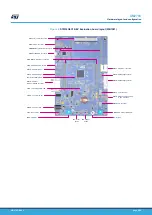
Страница 9: ...85 connector JP24 5 V Power jumper CN20 5 V Power jack LD1 4 User LEDs CN15 SWD debug connector CN14 SWD debug connector CN17 LCD connector CN18 Stereo audio jack 3 5mm with microphone CN19 LCD connector CN9 CN10 Extension connectors LD5 Low voltage alarm LED U7 STM32G0C1VET6 RV2 VDD ADJ B1 Reset button B2 Tamper button B3 Joystick RV3 VDD ANA potentiometer LD6 STLINK V2 1 COM LED UM2783 Hardware ...

Страница 10: ...rd LD1 IR LED D1 IR receiver Figure 6 UCPD daughterboard MB1352 CN7 USB Type C 1 DRP dual role port CN6 DisplayPortTM input CN4 USB 3 0 connector CN3 Extension power input CN2 DisplayPortTM output CN1 USB Type A CN5 USB Type C 2 sink UM2783 Hardware layout and configuration UM2783 Rev 1 page 10 59 ...

Страница 11: ...l SWD connector 6 1 1 Drivers Before connecting the STM32G0C1E EV Evaluation board to a Windows PC 7 8 or 10 through a USB a driver for the ST LINK V2 1 must be installed It is available on the www st com website In case the STM32G0C1E EV Evaluation board is connected to the PC before the driver is installed some STM32G0C1E EV interfaces may be declared as unknown in the PC device manager To recov...

Страница 12: ...ghterboard uses its own 19 V power adapter to support USB PD In this case the mother board uses D5V from the UCPD daughterboard to supply all circuits on the STM32G0C1E EV Evaluation board D5V of the UCPD daughterboard has three sources as below 19 V DC power adapter connected to MB1352_CN3 on the UCPD daughterboard Power from USB Type C port1 MB1352_CN7 on the UCPD daughterboard Power from USB Ty...

Страница 13: ...00 mA current If the host PC is not able to provide the requested current the enumeration fails Therefore the STM32 part including the extension board is not powered As a consequence the LD7 green LED remains turned OFF In this case it is mandatory to use an external power supply to supply extra power E5V from PSU or D5V can be used as an external power supply in case the current consumption of th...

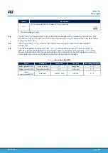
Страница 14: ...CN5 there is no USB enumeration needed The user can set JP24 to VUSB to allow the board to be powered anyway from CN5 The power source is selected by setting the JP24 JP16 and JP17 related jumpers as described in Table 4 Table 4 Power source related jumpers Jumper Description 1 JP24 For 5 V power supply from USB CN5 of ST LINK V2 1 through STMPS2141STR power switch with OVC protection to the STM32...

Страница 15: ...oard works with VDD 3 3 V so it is mandatory to close JP17 pin1 and pin2 The LED LD7 is lit when the STM32G0C1E EV Evaluation board is powered by the 5 V correctly Table 5 shows the low voltage limitations that may apply depending on the characteristics of some peripheral components Components may work incorrectly when the power level is lower than the limitation Table 5 Low voltage limitation Boa...

Страница 16: ... Table 7 8 MHz crystal X3 related solder bridges Solder bridge Description SB55 PF0 is connected to an 8 MHz crystal when SB55 is OFF PF0 is connected to the CN10 extension connector when SB55 is ON In such a case R46 must be removed to avoid disturbance due to the 8 Mhz quartz SB54 PF1 is connected to an 8 MHz crystal when SB54 is OFF PF1 is connected to the CN10 extension connector when SB54 is ...

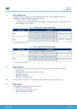
Страница 17: ...M32G0C1E EV Evaluation board boot from embedded SRAM CN10 pins 8 and 6 closed by jumper 1 STM32G0C1E EV Evaluation board boot from system memory 1 The default setting is in bold Table 9 Boot0 related jumper Solder bridge Description 1 JP2 PA14 BOOT0 is used as SWCLK when JP2 is set as shown here The Bootloader_BOOT0 is managed by pin 6 of the CN16 connector RS 232 DSR signal and it is connected to...

Страница 18: ...of the audio amplifier when JP23 is OFF JP19 Mono playback is enabled when JP19 is set as shown here Stereo playback is enabled when JP19 is set as shown here 1 The default setting is in bold The audio amplifier operates correctly when VDD is superior to 2 2 V and the microphone amplifier operates correctly when VDD is superior to 2 7 V 6 6 2 RS 232 and RS 485 Communication through RS 232 With Har...

Страница 19: ...wn here CN1 motor control connector must be OFF in this case 1 The default setting is in bold The RS 485 communication is supported by the ST3485EBDR RS 485 transceiver which is connected to pin 4 and pin 9 of D type 9 pins CN16 connector and shares the same connector with USART1 Table 12 RS 485 related jumpers Jumper Description 1 SB29 SB31 The external failsafe biasing is enabled when the SB29 a...

Страница 20: ...g board Available signals on this connector include emergency stop motor speed 3 phase motor current bus voltage power heatsink temperature coming from the motor driving board and six channels of PWM control signal going to the motor driving circuit The daughterboard on CN2 and CN3 must be removed and some jumpers set for motor control application JP5 JP6 and JP7 jumpers ON JP22 and JP19 jumpers O...

Страница 21: ...C IN1 as shown in Figure 9 on the STM32G0C1E EV Evaluation board Figure 9 GP comparator 1 band gap 1 2 V GPCOMP1_IN GPCOMP1_IN GND NC GP comparator 1 PA1 0 Ω LDR 8 2 KΩ ADC IN1 band gap band gap band gap DAC1 OUT VDDA It is possible to compare LDR output with 1 4 band gap 1 2 band gap 3 4 band gap band gap and DAC1 OUT and to connect LDR output to ADC IN1 for AD conversion 6 7 2 Temperature sensor...

Страница 22: ... 1 8 V operation and overrides any setting on the 5V 3V pin PA3 The smartcard operates correctly when VDD is higher than 2 7 V 6 7 4 HDMI CEC MB1351_CN1 and MB1351_CN3 HDMI connectors are available on the STM32G0C1E EV legacy peripheral daughterboard 1 The connector MB1351_CN1 is an HDMI sink connector with DDC connected to I2C2 of MCU HPD controlled by PD2 I O through MB1351_T1 transistor CEC con...

Страница 23: ...ation Port 2 can only be used as a sink Video signals on the MB1352_CN6 display port input connector and data signals on the MB1352_CN4 USB3 1 Gen1 Type B connector are multiplexed on USB Type C port 1 thanks to a TUSB546 DCI crosspoint switch IC These signals on MB1352_CN6 or MB1352_CN4 have to be generated by an external computer or notebook to evaluate the alternate mode AM capability of the US...

Страница 24: ...hterboard is generated from VBUS on port 2 when MB1352_JP5 is set as shown here 1 The default setting is in bold 6 8 3 VBUS management and discharge mechanism The MB1352_CN7 USB Type C port1 can be used as DRP dual role port Its VBUS can be managed for supplying other platforms as a provider or supplied as a consumer The MB1352_T6 and MB1352_T7 MOSFETs are set in back to back configuration to prot...

Страница 25: ...B1352_U17 and MB1352_U16 OVP chips This function is also embedded in MCU When the U17 OVP part is bypassed the dead battery function in MCU can be enabled or disabled through enabling signals by setting MB1352_JP2 CC1 or MB1352_JP1 CC2 Refer to Table 20 for detail Table 20 Dead battery related jumpers Jumper Description 1 MB1352_JP1 Embedded dead battery function is enabled when MB1352_JP1 is set ...

Страница 26: ...t and device Both USB Type C connectors are connected through MB1352_CN10 and MB1581_CN8 to MCU USB 2 0 FS interface through PA11 DM and PA12 DP UM2783 USB C and Power Delivery daughterboard MB1352 UM2783 Rev 1 page 26 59 ...

Страница 27: ...ion Emergency STOP PB12 1 2 GND PWM UH PA8 3 4 GND PWM UL PD2 5 6 GND PWM VH PA9 7 8 GND PWM VL PD3 9 10 GND PWM WH PA10 11 12 GND PWM WL PD4 13 14 PA1 BUS VOLTAGE PHASE A CURRENT PA2 15 16 GND PHASE B CURRENT PA6 17 18 GND PHASE C CURRENT PB10 19 20 GND NTC BYPASS RELAY PB9 21 22 GND DISSIPATIVE BRAKE PWM PB15 23 24 GND 5V power 25 26 PA3 Heatsink temperature PFC SYNC2 PD0 27 28 3 3V power PFC SY...

Страница 28: ...CN9 C10 extension connectors Each pin on CN2 and CN3 can be used by a daughterboard after disconnecting it from the corresponding function block on the STM32G0C1E EV Evaluation board Refer to Table 23 and Table 24 for details Table 23 CN2 daughterboard connector Pin Signal Mother board function Legacy daughterboard function MB1351_CN5 UCPD daughterboard function MB1352_CN9 How to disconnect with f...

Страница 29: ...ction MB1351_CN4 UCPD daughterboard function MB1352_CN8 How to disconnect with function block on mother board 1 PA8 MC_UH PORT1_CC1 2 PB15 MC_Dissipativebrake SmartCard 3 V 5 V PORT1_CC2 3 PA9 MC_VH USART1_TX_BOOT PORT1_DB1 Keep JP15 pin2 3 OFF 4 PA10 MC_WH USART1_RX_BOOT PORT1_DB2 Keep JP13 pin2 3 OFF 5 GND 6 PD4 MC_WL SmartCard CK VCONN_EN1 7 PB9 MC_NTC IR_OUT VCONN_EN2 8 PA2 MC_Current A SmartC...

Страница 30: ...ction MB1352_CN10 How to disconnect with function block on mother board 1 PA12 USART1_RTS C1_D Keep JP3 OFF 2 PA11 USART1_CTS_3V3 C1_D Keep JP4 OFF 3 PA12 USART1_RTS C2_D Keep JP3 OFF 4 PA11 USART1_CTS_3V3 C2_D Keep JP4 OFF 7 1 5 CN5 ST LINK V2 1 USB Micro B connector The CN5 USB Micro B connector is used to connect embedded ST LINK V2 1 to the PC for debugging of the board Figure 12 CN5 USB Micro...

Страница 31: ...een CN9 pin1 and CN10 pin1 is 2700 mils 68 58 mm The standard is implemented on the majority of evaluation boards Each pin on CN9 and CN10 can be used by a daughterboard after disconnecting it from the corresponding function block on STM32G0C1E EV Evaluation board Refer to Table 28 and Table 29 for details Table 28 CN9 extension connector Pin Description Alternative function How to disconnect with...

Страница 32: ... GND 12 PD1 MicroSD_CS_OD Remove SB14 14 PD6 LED2 Remove SB17 16 PF9 18 PF11 20 PF12 22 PB4 SPI1_MISO Remove SB19 24 PC10 VCP_TX STLINK RX Remove SB37 26 PE1 FDCAN2_STBY Remove SB21 28 PE2 30 GND 32 PE6 34 PC12 SPI1_MOSI_DIR Remove SB23 36 PC15 OSC32_OUT Fit SB52 Remove R40 38 PC8 JOY_LEFT Remove SB59 40 3V3 Table 29 CN10 extension connector Pin Description Alternative function How to disconnect w...

Страница 33: ... 39 GND 2 PA11 USB_FS_N Fit SB8 Remove SB6 Open JP4 4 PD10 6 PD8 LED3 Remove SB44 8 PE15 10 GND 12 PE12 14 PE10 16 PE8 18 PE7 20 PF7 22 PB2 Potentiometer VREF Remove SB45 24 PC4 USART1_TX Open JP15 26 PA6 Audio_IN Open JP22 Do not connect anything to CN1 28 PA4 Audio_OUT_L Open JP23 JP19 30 GND 32 PA0 JOY_SEL Remove SB56 34 PF3 Fit SB27 36 PC0 GPIO_EXT_RST Remove R11 Do not connect anything to CN4...

Страница 34: ...TS PA12 3 RS232_TX PC4 or PA9 8 RS232_CTS PA11 bootloader_RESET 4 RS485_A 9 RS485_B 7 1 10 CN14 SWD standard connector Figure 15 CN14 SWD standard connector top view 19 20 18 17 15 16 13 14 11 12 10 9 8 7 6 5 4 3 1 2 Table 31 CN14 SWD debugging connector Pin number Description Pin number Description 1 VDD 2 VDD 3 NC 4 GND 5 NC 6 GND 7 SWDAT PA13 8 GND 9 SWCLK PA14 10 GND UM2783 Connectors on mothe...

Страница 35: ... 32 CN15 high density SWD debugging connector Pin number Description Pin number Description 1 VDD 2 SWDAT PA13 3 GND 4 SWCLK PA14 5 GND 6 NC 7 KEY 8 NC 9 GND 10 RESET 7 1 12 CN17 CN19 TFT LCD connector A TFT colored LCD board is mounted on CN17 CN19 Refer to Section 6 6 7 for detail 7 1 13 CN18 audio jack A CN18 3 5 mm stereo audio jack connected to audio DAC and ADC is available on the STM32G0C1E...

Страница 36: ... 7 1 15 CN21 analog input connector Figure 18 CN21 analog I O connector top view 2 1 Table 33 CN21 analog I O connector Pin number Description Pin number Description 1 Analog I O PB2 2 GND 7 1 16 CN12 and CN13 CAN FD connectors Figure 19 CN12 and CN13 CAN FD connectors top view 2 1 Table 34 CN12 FDCAN1 connector Pin number Description 1 CAN1H 2 CAN1L Table 35 CN13 FDCAN2 connector Pin number Descr...

Страница 37: ... front view Table 36 MB1351_CN1 HDMI sink connector Pin number Description Pin number Description 1 3 4 6 7 9 10 12 TMDS differential signal pair connected to MB1351_CN3 16 I2C2_SDA PB14 13 CEC PB10 2 5 8 11 17 GND 14 NC 18 HDMI_5V_Sink 15 I2C2_SCL PB13 19 HPD PD2 through transistor UM2783 Connectors on the legacy peripheral daughterboard MB1351 UM2783 Rev 1 page 37 59 ...

Страница 38: ...onnector Pin number Description Pin number Description 1 VCC 5 GND 2 RST 6 NC 3 CLK 7 I O 4 NC 8 NC 17 Card presence detection pin 18 Card presence detection pin 7 2 3 MB1351_CN3 HDMI source connector Figure 22 MB1351_CN3 HDMI source connector front view UM2783 Connectors on the legacy peripheral daughterboard MB1351 UM2783 Rev 1 page 38 59 ...

Страница 39: ...n the legacy daughterboard is connected to CN3 on the mother board and CN5 on the legacy daughterboard is connected to CN2 on the mother board Refer to Section 7 1 3 for a detailed signal definition of these connectors 7 3 Connectors on UCPD daughterboard MB1352 7 3 1 MB1352_CN1 USB Type A connector Figure 23 MB1352_CN1 USB Type A connector front view Table 39 MB1352_CN1 USB Type A connector Pin n...

Страница 40: ...N 2 5 8 11 16 GND 7 3 3 MB1352_CN3 19 V Power connector The UCPD daughterboard can be powered from a DC 19 V power supply via the MB1352_CN3 external power supply jack as shown in Figure 25 And it is used for USB Power Delivery Figure 25 MB1352_CN3 Power connector front view 7 3 4 MB1352_CN4 USB3 1 Gen1 Type B connector Figure 26 MB1352_CN4 USB3 1 Gen1 Type B connector front view UM2783 Connectors...

Страница 41: ...or Figure 27 PORT2 MB1352_CN5 USB Type C connector front view Table 42 PORT2 MB1352_CN5 USB Type C connector Pin number Description Pin number Description A1 GND B1 GND A2 TX1 B2 TX2 A3 TX1 B3 TX2 A4 VBUS B4 VBUS A5 CC1 PD0 B5 CC2 PD2 A6 D B6 D A7 D B7 D A8 SBU1 B8 SBU2 A9 VBUS B9 VBUS A10 RX2 B10 RX1 A11 RX2 B11 RX1 A12 GND B12 GND UM2783 Connectors on UCPD daughterboard MB1352 UM2783 Rev 1 page ...

Страница 42: ...NFIG2 4 LANE2_N 15 AUX_CH_P 6 LANE2_P 17 AUX_CH_N 7 LANE1_N 18 HPD PB5 9 LANE1_P 19 RETURN 10 LANE0_N 20 DP_PWR 12 LANE0_P 2 5 8 11 16 GND 7 3 7 PORT1 MB1352_CN7 USB Type C connector Figure 29 PORT1 MB1352_CN7 USB Type C connector front view Table 44 PORT1 MB1352_CN7 USB Type C connector Pin number Description Pin number Description A1 GND B1 GND A2 TX1 B2 TX2 UM2783 Connectors on UCPD daughterboa...

Страница 43: ...on the USB C daughterboard is connected to CN3 on the mother board and MB1352_CN9 on the USB C daughterboard is connected to CN2 on the mother board Refer to Section 7 1 3 for a detailed signal definition of these connectors 7 3 9 MB1352_CN10 USB 2 0 FS board to board connector One female connector MB1352_CN10 is used to connect the mother board USB 2 0 FS data interface DP DM to USB Type C daught...

Страница 44: ...32 marking refer to the STM32 datasheet Package information paragraph at the www st com website Next to the evaluation tool ordering part number that is stuck or silk screen printed on the board Some boards feature a specific STM32 device version which allows the operation of any bundled commercial stack library available This STM32 device shows a U marking option at the end of the standard part n...

Страница 45: ...24 RV3 VDD_ANA instead of ADC ref CN21 AIN instead of Analog I O CN20 PSU 5 V E5V No workaround 92534 ST Link I O level shifter must be connected to 3V3_STLK instead of 3V3 No workaround 8 3 2 MB895 LCD daughterboard Revision C03 No known limitations 8 3 3 MB1351 legacy peripheral daughterboard Revision A01 No known limitations 8 3 4 MB1352 USB C daughterboard Revision C03 No known limitations UM2...

Страница 46: ...FP VREFP 13 VDD_1 VDD 14 VSS_1 GND 15 PF0 OSC_IN OSC_IN 16 PF1 OSC_OUT OSC_OUT 17 PF2 NRST NRST WKUP8 18 PF3 FREE 19 PF4 FREE 20 PF5 FREE 21 PC0 GPIO_EXT_RST 22 PC1 MC_IO_ PFC_sync1 GPIO_9V_EN_LPTIM1_OUT 23 PC2 GPIO_JOY_UP 24 PC3 GPIO_JOY_DOWN 25 PA0 JOY_SEL_TAMP_IN2 WKUP1 26 PA1 MC_AIN1_COMP_1_INP Bus voltage LDR_OUT_COMP_1_INP_A DC_IN1 GPIO_15V_EN_DCDC_EN 27 PA2 MC_ADC_IN2 CurrentA SMART_2_TX TY...

Страница 47: ...5 BOARD_DET_ADC_IN15 51 PB12 MC_TIM_1_BK Emergency STOP GPIO_SMART_OFF TYPE C_2_I_ADC_IN16 52 PB13 I2C2_SCL HDMI_SINK GPIO_DISCHARGE_1 53 PB14 I2C2_SDA HDMI_SINK GPIO_DISCHARGE_2 54 PB15 MC_IO_ Dissipative brake GPIO_SMART_3V or GPIO_SMART_5V TYPE C_1_CC2 55 PA8 MC_TIM_1_CH1 UH TYPE C_1_CC1 56 PA9 USART_BOOT_1_TX MC_TIM_1_CH2 VH TYPE C_1_DBCC1 57 PC6 MC_TIM_3_CH1 EncoderA IR_IN_TIM3_CH1 GPIO_DP2_H...

Страница 48: ...HDMI_HPD_SINK TYPE C_2_CC2 81 PD3 MC_TIM_1_CH2N VL GPIO_HDMI_HPD_SOURCE GPIO_SOURCE_EN 82 PD4 MC_TIM_1_CH3N WL SMART_2_RTS_DE_CK GPIO_VCONN_EN_1_1 83 PD5 LED1 84 PD6 LED2 85 PD7 FREE 86 PF9 FREE 87 PF10 FREE 88 PF11 FREE 89 PF12 FREE 90 PF13 FREE 91 PB3 LCD SD1_SCK 92 PB4 LCD SD1_MISO 93 PB5 MC_TIM_3_CH2 EncoderB TEMP_SENSOR_INT_WKUP 6 GPIO_DP1_DET 94 PE0 FDCAN1_STBY 95 PE1 FDCAN2_STBY 96 PE2 FREE...

Страница 49: ...al dimensions Symbol Size in millimeters Symbol Size in millimeters Symbol Size in millimeters A 68 58 e 77 44 P2 111 76 A1 61 97 H 11 P3 10 41 a 2 54 Lx 5 715 Q1 24 12 B 36 Ly 5 715 Q2 17 70 D 3 5 Mx 19 08 Q3 16 d 3 2 My 18 73 X 114 3 E 47 P1 60 71 Y 172 72 UM2783 STM32G0C1E EV mechanical dimensions UM2783 Rev 1 page 49 59 ...

Страница 50: ...onsible party in the USA Terry Blanchard Americas Region Legal Group Vice President and Regional Legal Counsel The Americas STMicroelectronics Inc 750 Canyon Drive Suite 300 Coppell Texas 75019 USA Telephone 1 972 466 7845 C 2 ISED Compliance Statement This device complies with FCC and ISED Canada RF radiation exposure limits set forth for general population for mobile application uncontrolled exp...

Страница 51: ... cet équipement peut créer des interférences radio D 2 Simplified declaration of conformity Hereby STMicroelectronics declares that the STM32G0C1E EV Evaluation board with STM32G0C1VE MCU comply with the applicable CE requirements stated below EN 55032 2012 2015 EN 55035 2017 EN 60950 1 2006 A11 2009 A1 2010 A12 2011 A2 2013 EN 62368 1 2014 A1 2017 CFR 47 FCC Part 15 B ICES 003 Issue 6 2016 The co...

Страница 52: ...Revision history Table 49 Document revision history Date Revision Changes 1 Dec 2020 1 Initial release UM2783 UM2783 Rev 1 page 52 59 ...

Страница 53: ...firmware upgrade 11 6 2 Power supply 12 6 3 Clock references 16 6 4 Reset sources 16 6 5 Boot option 16 6 6 Peripherals on mother board MB1581 18 6 6 1 Audio 18 6 6 2 RS 232 and RS 485 18 6 6 3 microSD card 19 6 6 4 Analog input 20 6 6 5 External I2C connector 20 6 6 6 Motor control 20 6 6 7 Display and input devices 20 6 6 8 CAN FD 21 6 7 Peripherals on the legacy peripheral daughterboard MB1351 ...

Страница 54: ...ector 30 7 1 5 CN5 ST LINK V2 1 USB Micro B connector 30 7 1 6 CN6 ST LINK V2 1 programming connector 30 7 1 7 CN11 microSD connector 31 7 1 8 CN9 and CN10 extension connectors 31 7 1 9 CN16 RS 232 and RS 485 connector 34 7 1 10 CN14 SWD standard connector 34 7 1 11 CN15 high density SWD debugging connector 35 7 1 12 CN17 CN19 TFT LCD connector 35 7 1 13 CN18 audio jack 35 7 1 14 CN20 5 V power co...

Страница 55: ...8 2 Board revision history 44 8 2 1 MB1581 mother board 44 8 2 2 MB895 LCD daughterboard 44 8 2 3 MB1351 legacy peripheral daughterboard 44 8 2 4 MB1352 USB C daughterboard 44 8 3 Known limitations 45 8 3 1 MB1581 mother board 45 8 3 2 MB895 LCD daughterboard 45 8 3 3 MB1351 legacy peripheral daughterboard 45 8 3 4 MB1352 USB C daughterboard 45 Appendix A STM32G0C1E EV I O Assignment 46 Appendix B...

Страница 56: ...Revision history 52 Contents 53 List of tables 57 List of figures 58 UM2783 Contents UM2783 Rev 1 page 56 59 ...

Страница 57: ...rboard connector 29 Table 25 CN8 USB 2 0 FS board to board connector 30 Table 26 CN5 USB Micro B connector pinout 30 Table 27 CN11 microSD connector 31 Table 28 CN9 extension connector 31 Table 29 CN10 extension connector 32 Table 30 CN16 RS 232 and RS 485 connector 34 Table 31 CN14 SWD debugging connector 34 Table 32 CN15 high density SWD debugging connector 35 Table 33 CN21 analog I O connector ...

Страница 58: ...ector top view 34 Figure 16 CN15 high density SWD debugging connector top view 35 Figure 17 CN20 power supply connector front view 36 Figure 18 CN21 analog I O connector top view 36 Figure 19 CN12 and CN13 CAN FD connectors top view 36 Figure 20 MB1351_CN1 HDMI sink connector front view 37 Figure 21 MB1351_CN2 smartcard connector top view 38 Figure 22 MB1351_CN3 HDMI source connector front view 38...

Страница 59: ...cts and ST assumes no liability for application assistance or the design of Purchasers products No license express or implied to any intellectual property right is granted by ST herein Resale of ST products with provisions different from the information set forth herein shall void any warranty granted by ST for such product ST and the ST logo are trademarks of ST For additional information about S...

Отзывы: