


Recommended PCB routing guidelines for STM32F4xxxx devices
AN4488
38/50
AN4488 Rev 7
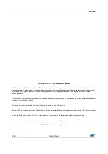
Figure 23. Typical layout for V
DD
/V
SS
pair
8.4
High speed signal layout
8.4.1
SDMMC bus interface
Interface connectivity
The SD/SDIO MMC card host interface (SDMMC) provides an interface between the APB2
peripheral bus and Multi Media Cards (MMCs), SD memory cards and SDIO cards. The
SDMMC interface is a serial data bus interface, that consists of a clock (CK), command
signal (CMD) and 8 data lines (D [0:7]).
Interface signal layout guidelines:
•
Reference the plane using GND or PWR (if PWR, add 10nf switching cap between
PWR and GND)
•
Trace the impedance: 50
Ω
± 10%
•
The skew being introduced into the clock system by unequal trace lengths and loads,
minimize the board skew, keep the trace lengths equal between the data and clock.
•
The maximum skew between data and clock should be below 250 ps @ 10mm
•
The maximum trace length should be below 120mm. If the signal trace exceeds this
trace-length/speed criterion, then a termination should be used
•
The trace capacitance should not exceed 20 pF at 3.3V and 15pF at 1.8V
•
The maximum signal trace inductance should be less than 16nH
•
Use the recommended pull-up resistance for CMD and data signals to prevent bus
floating.
•
The mismatch within data bus, data and CK or CK and CMD should be below 10mm.
•
Keep the same number of vias between the data signals
Note:
The total capacitance of the SD memory card bus is the sum of the bus master capacitance.
CHOST, the bus capacitance CBUS itself and the capacitance CCARD of each card
connected to this line. The total bus capacitance is CL= CHost + CBus + N*CCard where
Host is STM32F4xxxx, bus is all the signals and Card is SD card.
sŝĂƚŽs
sŝĂƚŽs^^
ss^^
ĂƉ͘
069
^dDϯϮ&ϰdždž
ĂƉ͘


