background image

AN4

488

Ref
e

ren
ce de

sign

AN44

88 Rev 7

35

/50

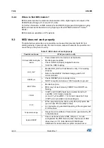
Figure 20. Bill of Material

Comment

Description

Designator

Footprint

Quantity

TD-0341  [RESET/Black]

SE  PUSHBUTTON

B1

PB10

1

CR1220  holder

Battery

BT1

BAT_2SM_CR1220

1

100nF

Capacitor

C1,  C2,  C3,  C4,  C5,  C6,  C7, 
C8,  C9,  C13,  C14,  C15,  C16, 
C17,  C18,  C19,  C20,  C21, 
C22,  C23,  C25,  C30

0402C

22

4.7uF

Polarized  Capacitor  (Radial)

C10,  C11

TAN-A

2

1uF

Polarized  Capacitor  (Radial)

C12,  C24

TAN-A

2

2.2uF

Capacitor

C26,  C27

1206C

2

2.2uF[N/A]

Capacitor

C28

1206C

1

2.2uF

Capacitor

C29

0402C

1

100nF

Capacitor

C31

0603C

1

20pF

Capacitor

C32,  C33

0603C

2

1.5pF

Capacitor

C34,  C35

0603C

2

JTAG

CN1

IDC20S

1

JP10

SIP3

1

BEAD(FCM1608KF-601T03)

Inductor

L1

0603L

1

10K

Resistor

R1,  R2,  R3,  R4,  R8,  R9,  R12

0603R

7

0

Resistor

R5,  R6,  R7,  R11

0603R

4

[N/A]

Resistor

R10

0603R

1

09.03290.01

SPDT  Subminiature  Toggle 
Switch,  Right  Angle 
Mounting,  Vertical 
Actuation

SW1,  SW2

SW1_3TH_2R54_10X2R5

2

STM32F469

U1

BGA216_0R8_13X13_SKT

1

25MHz(with  socket)

Crystal

X1

XTAL_socket

1

NX3215SA-32.768KHZ-EXS00A Crystal

X2

XTAL_2SM_3R2X1R5

1

Содержание STM32F4 Series

Страница 1: ...gh performance microcontrollers listed in Table 1 and describes the minimum hardware resources required to develop an application based on those products Detailed reference design schematics are also contained in this document together with descriptions of the main components interfaces and modes Table 1 Applicable products Type Part numbers and Product lines Microcontrollers STM32F401xB STM32F401...

Страница 2: ...y example 15 3 2 2 Power on reset POR power down reset PDR 17 3 2 3 Programmable voltage detector PVD 18 4 Package 20 4 1 Package Selection 20 4 2 Pinout Compatibility 22 4 2 1 I O speed 22 4 3 Alternate Function 24 4 3 1 Handling unused pins 25 4 4 Boot mode selection 25 4 4 1 Boot mode selection 25 4 5 Boot pin connection 27 4 6 Embedded boot loader mode 27 5 Debug management 29 5 1 SWJ debug po...

Страница 3: ... 1 SDMMC bus interface 38 8 4 2 Flexible memory controller FMC interface 39 8 4 3 Quadrature serial parallel interface Quad SPI 39 8 4 4 Embedded trace macrocell ETM 40 8 5 Package layout recommendation 41 8 5 1 BGA 216 0 8 mm pitch design example 41 8 5 2 WLCSP143 0 4 mm pitch design example 42 9 FAQ 45 9 1 Identify the STM32F4xxxx 45 9 2 Hardware tools available 45 9 2 1 Nucleao Boards 45 9 2 2 ...

Страница 4: ... AC characteristics 22 Table 5 Alternate function 24 Table 6 Boot modes 26 Table 7 STM32F4xxxx bootloader communication peripherals 27 Table 8 Debug port pin assignment 30 Table 9 BGA 216 0 8 mm pitch package information 41 Table 10 Wafer level chip scale package information 42 Table 11 MCU does not work properly 46 Table 12 Document revision history 48 ...

Страница 5: ...t to scale not needed for STM32F410xx STM32F411xx STM32F412xx STM32F413xx STM32F423xx STM32F446xx STM32F469xx and STM32F479xx 17 Figure 9 Power on reset power down reset waveform 18 Figure 10 PVD thresholds 19 Figure 11 STM32CubeMX example screen shot 25 Figure 12 Boot mode selection implementation example 27 Figure 13 Host to board connection 29 Figure 14 JTAG connector implementation 31 Figure 1...

Страница 6: ... a based devices Table 2 Referenced documents Reference Title AN2867 Oscillator design guide for ST microcontrollers AN2606 STM32 microcontroller system memory boot mode AN3364 Migration and compatibility guidelines for STM32 microcontroller applications a Arm is a registered trademark of Arm Limited or its subsidiaries in the US and or elsewhere ...

Страница 7: ...rs and SRAM in Standby mode the regulator is powered down The contents of the registers and SRAM are lost except for those concerned with the Standby circuitry and the Backup domain Note Depending on the selected package there are specific pins that should be connected either to VSS or VDD to activate or deactivate the voltage regulator Refer to section Voltage regulator in datasheet for details 2...

Страница 8: ...ages In that case a single 100 nF decoupling capacitor is connected to VCAP1 The following conditions must be respected VDD should always be higher than VCAP to avoid current injection between power domains If the time for VCAP to reach V12 minimum value is smaller than the time for VDD to reach 1 7 V then PA0 should be kept low to cover both conditions until VCAP reaches V12 minimum value and unt...

Страница 9: ...ramic The VREF pin can be connected to the VDDA external power supply If a separate external reference voltage is applied on VREF a 100 nF and a 1 µF capacitors must be connected on this pin In all cases VREF must be kept between VDDA 1 2 V and VDDA with minimum of 1 7 V Additional precautions can be taken to filter analog noise VDDA can be connected to VDD through a ferrite bead The VREF pin can ...

Страница 10: ...REF is either connected to VREF or to VSSA depending on package 5 N is the number of VDD and VSS inputs 6 Refer to datasheet for BYPASS_REG and PDR_ON pins connection 7 VDDUSB is only available on STM32F446xx 8 Backup RAM is not available on STM32F410xx STM32F411xx STM32F412xx STM32F413xx and STM32F423xx 06Y 9 DFNXS FLUFXLWU 26 57 DNHXS ORJLF DFNXS UHJLVWHUV EDFNXS 5 0 HUQHO ORJLF 38 GLJLWDO 5 0 Q...

Страница 11: ...nding on package 3 VREF is either connected to VREF or to VSSA depending on package 4 Refer to datasheet for BYPASS_REG and PDR_ON pins connection 06Y 9 DFNXS FLUFXLWU 26 57 DNHXS ORJLF DFNXS UHJLVWHUV EDFNXS 5 0 HUQHO ORJLF 38 GLJLWDO 5 0 QDORJ 5 V 3 3RZHU VZLWFK 9 7 3 2V 287 1 Q 9 7 WR 9 9ROWDJH UHJXODWRU 9 HYHO VKLIWHU 2 RJLF 9 Q ODVK PHPRU 9 3B 9 3B î 3 66B5 3 5B21 5HVHW FRQWUROOHU 9 966 9 95 ...

Страница 12: ...n VDDA pin An isolated supply ground connection is provided on the VSSA pin In all cases the VSSA pin should be externally connected to same supply ground than VSS To ensure a better accuracy on low voltage inputs the user can connect a separate external reference voltage ADC input on VREF The voltage on VREF may range from VDDA 1 2 V to VDDA with a minimum of 1 7 V When available depending on pac...

Страница 13: ...t to power up correctly Only a pull down capacitor is recommended to improve EMS performance by protecting the device against parasitic resets as exemplified in Figure 4 Charging and discharging a pull down capacitor through an internal resistor increases the device power consumption The capacitor recommended value 100 nF can be reduced to 10 nF to limit this power consumption Figure 4 Reset circu...

Страница 14: ...tor PVD is disabled VBAT functionality is no more available and VBAT pin should be connected to VDD Figure 5 NRST circuitry example only for STM32F410xx STM32F411xx STM32F412xx STM32F413xx STM32F423xx STM32F446xx STM32F469xx and STM32F479xx Even with PDR_ON 0 during power up the NRST is driven low by internal Reset controller during TRSTTEMPO in order to allow stabilization of internal analog circ...

Страница 15: ...supervisor 3 2 1 PDR_ON circuitry example Note This example doesn t apply to STM32F410xx STM32F411xx STM32F412xx STM32F413xx STM32F423xx STM32F446xx STM32F469xx and STM32F479xx where PDR_ON can be connected to VSS to permanently disable internal reset circuitry external voltage supervisor required on NRST pin Thanks to backward compatibility circuitry built for other STM32F4xxxx products will work...

Страница 16: ... to drive PDR_ON 1 during power off sequence When the internal reset is OFF the following integrated features are no longer supported The integrated power on reset POR power down reset PDR circuitry is disabled The brownout reset BOR circuitry must be disabled The embedded programmable voltage detector PVD is disabled VBAT functionality is no more available and VBAT pin should be connected to VDD ...

Страница 17: ...8V 5 mean VDD min1 71V Supervisor specified at 1 66V 2 5 with an hysteresis of 0 5 mean rising trip max 1 71V 1 66V 2 5 0 5 falling trip min 1 62V 1 66V 2 5 3 2 2 Power on reset POR power down reset PDR The device has an integrated POR PDR circuitry that allows proper operation starting from 1 8 V The device remains in the Reset mode as long as VDD is below a specified threshold VPOR PDR without t...

Страница 18: ...isor See Section 3 2 1 for details 3 2 3 Programmable voltage detector PVD You can use the PVD to monitor the VDD power supply by comparing it to a threshold selected by the PLS 2 0 bits in the Power control register PWR_CR The PVD is enabled by setting the PVDE bit A PVDO flag is available in the Power control status register PWR_CSR to indicate whether VDD is higher or lower than the PVD thresho...

Страница 19: ...AN4488 Rev 7 19 50 AN4488 Reset and power supply supervisor 49 Figure 10 PVD thresholds 6 M6 HYSTERESIS 06 THRESHOLD 06 OUTPUT AI B 606 FALLING EDGE 606 RISING EDGE ...

Страница 20: ...Small pitch and high ball density requires multilayer PCBs which allow better supply ground distribution Compatibility with other devices Table 3 summarizes the available packages for all STM32F4xxxx family Table 3 Package summary Size mm 1 10 x 10 14 x 14 20 x 20 24 x 24 28 x 28 13 x 13 7 x 7 7 x 7 7 x 7 10 x 10 7 x 7 10 x 10 2 553 x 2 579 3 034 x 3 220 3 060 x 3 060 3 658 x 3 686 4 039 x 3 951 5...

Страница 21: ... mm 1 10 x 10 14 x 14 20 x 20 24 x 24 28 x 28 13 x 13 7 x 7 7 x 7 7 x 7 10 x 10 7 x 7 10 x 10 2 553 x 2 579 3 034 x 3 220 3 060 x 3 060 3 658 x 3 686 4 039 x 3 951 5 693 x 3 815 4 223 x 4 223 4 521 x 5 547 4 891 x 5 692 Sales numbers LQFP64 LQFP100 LQFP144 LQFP176 LQFP208 TFBGA216 UFQFPN48 UFBGA100 UFBGA144 UFBGA144 UFBGA169 UFBGA176 WLCSP36 WLCSP49 WLCSP49 WLCSP64 WLCSP81 WLCSP81 WLCSP90 WLCSP143...

Страница 22: ...2 OSPEEDR y 1 0 bit value 1 Symbol Parameter Conditions Min Typ Max Unit 00 fmax IO out Maximum frequency CL 50 pF VDD 2 7 V 4 MHz CL 50 pF VDD 1 7 V 2 CL 10 pF VDD 2 7 V 8 CL 10 pF VDD 1 8 V 4 CL 10 pF VDD 1 7 V 3 tf IO out tr IO out Output high to low level fall time and output low to high level rise time CL 50 pF VDD 1 7 V to 3 6 V 100 ns 01 fmax IO out Maximum frequency 3 CL 50 pF VDD 2 7 V 25...

Страница 23: ... Output high to low level fall time and output low to high level rise time CL 30 pF VDD 2 7 V 4 ns CL 30 pF VDD 1 8 V 6 CL 30 pF VDD 1 7 V 7 CL 10 pF VDD 2 7 V 2 5 CL 10 pF VDD 1 8 V 3 5 CL 10 pF VDD 1 7 V 4 tEXTIpw Pulse width of external signals detected by the EXTI controller 10 ns 1 Guaranteed by design 2 The I O speed is configured using the OSPEEDRy 1 0 bits Refer to the STM32F4xx reference ...

Страница 24: ... 5 TIM8 9 10 11 I2C1 2 3 SPI1 2 3 4 5 6 SPI2 3 SAI1 SPI2 3 USAR T1 2 3 USA RT6 UAR T4 5 CAN1 2 TIM12 13 14 QUAD QUADS PI OTG 2_HS O TG1_F ETH FMC SDIO OTG2 _ DCMI DSI HOST LCD SYS Port B PB0 TIM1_ CH2N TIM3_ CH3 TIM8_ CH2N LCD_R3 OTG_HS_ ULPI_D1 ETH_MII_ RXD2 LCD_ G1 EVENT OUT PB11 TIM2_ CH4 I2C2_ SDA USART3 _RX OTG_HS _ULPI_D4 ETH_MII_ TX_EN ETH_RMII_ TX_EN DSI HOST _TE LCD_ G5 EVENT OUT PB12 TIM...

Страница 25: ...ormance unused clocks counters or I Os should not be left free e g I Os should be set to 0 or 1 pull up or pull down to the unused I O pins and unused features should be frozen or disabled Note To reduce leakage it is advisable to configure the I O as an analog input or to push pull and to set it to 0 4 4 Boot mode selection 4 4 1 Boot mode selection In the STM32F4xxxx three different boot modes c...

Страница 26: ... not the user flash is now aliased to start at address 0x00000000 The application code in this case must have already been loaded into system memory Boot from Embedded SRAM mode The SRAM start at address 0x00000000 When this mode is selected the device expects the vector table to have been relocated using the NVIC exception table and offset register and execution begins at the start of embedded SR...

Страница 27: ...cation peripherals Bootloader peripherals STM32F401xB C STM32F401xD E STM32F405 415 STM32F407 417 STM32F427 437 STM32F429 439 STM32F410xx STM32F411xC STM32F411xE STM32F412xx STM32F413xx STM32F423xx STM32F469xx STM32F479xx DFU USB OTG FS PA11 12 in Device mode USB OTG FS PA11 12 in Device mode USB OTG FS PA11 12 in Device mode USB OTG FS PA11 12 in Device mode USB OTG FS PA11 12 in Device mode USAR...

Страница 28: ...C11 PC12 PA15 PC10 PC11 PC12 SPI4 PE11 PE12 PE13 PE14 Table 7 STM32F4xxxx bootloader communication peripherals continued Bootloader peripherals STM32F401xB C STM32F401xD E STM32F405 415 STM32F407 417 STM32F427 437 STM32F429 439 STM32F410xx STM32F411xC STM32F411xE STM32F412xx STM32F413xx STM32F423xx STM32F469xx STM32F479xx ...

Страница 29: ...provides a 5 pin standard JTAG interface to the AHP AP port The serial wire debug port SW DP provides a 2 pin clock data interface to the AHP AP port In the SWJ DP the two JTAG pins of the SW DP are multiplexed with some of the five JTAG pins of the JTAG DP For more details on the SWJ debug port refer to the reference manual of the product SWJ debug port section serial wire and JTAG 5 2 Pinout and...

Страница 30: ...p JTMS SWDIO Input pull up JTCK SWCLK Input pull down JTDO Input floating The software can then use these I Os as standard GPIOs Note The JTAG IEEE standard recommends to add pull up resistors on TDI TMS and nTRST but there is no special recommendation for TCK However for the STM32F4xxxx an integrated pull down resistor is used for JTCK Having embedded pull up and pull down resistors removes the n...

Страница 31: ...AN4488 Rev 7 31 50 AN4488 Debug management 49 Figure 14 JTAG connector implementation 06 9 9 9 670 Q 7567 7 670 6 2 7 6 7 2 Q567 1 975 Q7567 7 706 7 57 7 2 Q6567 54 N N N 966 RQQHFWRU î 7 FRQQHFWRU 1 ...

Страница 32: ...t is not used to optimize the power consumption Refer to the reference manual for the description of the clock tree 6 1 HSE OSC clock The high speed external clock signal HSE can be generated from two possible clock sources HSE user external clock see Figure 15 HSE external crystal ceramic resonator see Figure 16 1 The value of REXT depends on the crystal characteristics Typical value is in the ra...

Страница 33: ...crystal ceramic resonators figures OSC32_IN and OSC32_OUT pins can be used also as GPIO but it is recommended not to use them as both RTC and GPIO pins in the same application 3 LSE crystal ceramic resonators figure The value of REXT depends on the crystal characteristics A 0 Ω resistor would work but would not be optimal To fine tube RS value refer to AN2867 Oscillator design guide for ST microco...

Страница 34: ... 0 7 R D 0 7 D 0 9 7 R M0 9 7 0 0 9 7 0 0 0 9 7 0 0 9 7 0 0 9 7 0 0 7 0 9 0 7 0 0 7 0 0 0 7 0 0 7 0 7 R 7 9 7 7 L 9 7 L 7 R 7 0 O T M0 7 0 9 O T U D 0 7 F O T 0 7 F0 O T U F0 W 0 M 7 T M9 7 W 7 L 7 W 7 W R 7 W 9 0 T T 7 W 0 T AT 7 F0 T T W 0 T AT F0 7 W 0 0 7 W 0 R 7 W 0 R 7 W 0 9 0 7 W 7 W 0 L T 0 T D 0 7 A 7 A L 7 A9 7 A 9 7 AL T 0 T 7 D 0 U0 D R S 0 S D 0 S 0 AR S MD O 0 S 0 S MD X 7 0 S 0 D S ...

Страница 35: ... 2 2 2uF Capacitor C26 C27 1206C 2 2 2uF N A Capacitor C28 1206C 1 2 2uF Capacitor C29 0402C 1 100nF Capacitor C31 0603C 1 20pF Capacitor C32 C33 0603C 2 1 5pF Capacitor C34 C35 0603C 2 JTAG CN1 IDC20S 1 JP10 SIP3 1 BEAD FCM1608KF 601T03 Inductor L1 0603L 1 10K Resistor R1 R2 R3 R4 R8 R9 R12 0603R 7 0 Resistor R5 R6 R7 R11 0603R 4 N A Resistor R10 0603R 1 09 03290 01 SPDT Subminiature Toggle Switc...

Страница 36: ...uired impedances to be realized The minimum configuration that can be used is 4 or 6 layers stack up An 8 layers boards may be required for a very dense PCBs that have multiple SDRAM SRAM NOR LCD components The following stack ups are intended as examples which can be used as a starting point for helping in a stack up evaluation and selection These stack up configurations are using a GND plane adj...

Страница 37: ...d with thick track widths and preferably the use of dedicated power supply planes in multilayer PCBs In addition each power supply pair should be decoupled with filtering Ceramic capacitors 100 nF and one single Tantalum or Ceramic capacitor min 4 7 µF typ 10 µF connected in parallel These capacitors need to be placed as close as possible to or below the appropriate pins on the underside of the PC...

Страница 38: ...ngths equal between the data and clock The maximum skew between data and clock should be below 250 ps 10mm The maximum trace length should be below 120mm If the signal trace exceeds this trace length speed criterion then a termination should be used The trace capacitance should not exceed 20 pF at 3 3V and 15pF at 1 8V The maximum signal trace inductance should be less than 16nH Use the recommende...

Страница 39: ...s trace length speed criterion then a termination should be used Reduce the crosstalk place data tracks on the different layers from the address and control lanes if possible Ho wever when the data and address control tracks coexist on the same layer they must be isolated from each other by at least 5 mm Match the trace lengths for the data group within 10 mm of each other to diminish the skew Ser...

Страница 40: ... serpentine routing for the clock signal and as less via s as possible for the whole path a via alter the impedance and add a reflection to the signal 8 4 4 Embedded trace macrocell ETM Interface connectivity The ETM enables the reconstruction of the program execution The data are traced using the data watchpoint and trace DWT component or the instruction trace macrocell ITM whereas instructions a...

Страница 41: ... without fan out via The current pitch size allows to route only one trace between two adjacent BGA land pads Figure 26 shows an example of ideal SDRAM signals fan out vias with power and gnd signals These signals can be optimized to achieve the routing and length matching in an another layer before connecting to an SDRAM IC Figure 24 BGA 0 8mm pitch example of fan out Table 9 BGA 216 0 8 mm pitch...

Страница 42: ... 9LD 9LD ULOO 3DG WR YLD VSDFH 7UDFH 06Y 9 0 1 3 5 3 5 1 0 Table 10 Wafer level chip scale package information Package information mm Design parameters mm Bump pitch 0 4 Microvia size hole size 0 1 via land 0 2 Bump size 0 25 Trace width space 0 07 0 05 or 0 07 0 07 Number of rows columns 13x11 Bump pad size 0 26 max 0 22 recommended Non solder mask defined via underbump allowed Solder mask openin...

Страница 43: ...e out internal bumps to a buried layers inside the PCB To achieve this the WLCSP package pads have to be connected to this internal layer through microvia In case of four layers PCB the first layer is WLCSP component the second layer will be used as a signal layer the third layer as the power and ground and the bottom layer for a signal layout Figure 27 shows an example of the layout for four laye...

Страница 44: ...ting guidelines for STM32F4xxxx devices AN4488 44 50 AN4488 Rev 7 Figure 27 143 bumps WLCSP 0 40 mm pitch routing example 06Y 9 3 5 1 6LJQDOV D HU D HU 3 5 1 3 5 1 6LJQDOV 0 1 D HU 7RS D HU 6LJQDOV 6LJQDOV 0LFURYLD 3 5 1 ...

Страница 45: ...y be expanded through a variety of add on boards 9 2 2 Discovery kits Discovery boards helps user to discover the high performance microcontrollers of the STM32 F4 series and to develop applications easily Different discovery boards are available For example the STM32F429I DISCO includes these features SDRAM 64Mbits L3GD20 MEMS motion sensor 3 axis digital output gyroscope USB OTG with micro AB co...

Страница 46: ...GND is properly supplied to device Verify the GND coupling OSC_OUT Monitor OSC_OUT with oscillator to verify if it is working properly Refer to the AN2867 Oscillator design guide for ST microcontrollers RESET pin Check if RESET pin is correctly driven NRST connection includes a 100nF capacitor to ground BOOT PINs Monitor boot pins MCU may not work properly if BOOT0 and BOOT1 are floating VCAPs VCA...

Страница 47: ...AN4488 Rev 7 47 50 AN4488 Conclusion 49 10 Conclusion This application note should be used as a starting reference for a new design with STM32F4xxxx device ...

Страница 48: ...family compatible board design for LQFP64 package Figure 10 STM32F4 family compatible board design for LQFP100 package Figure 12 Compatible board design STM32F10xx STM32F4xx for LQFP64 package Figure 13 Compatible board design STM32F10xx STM32F2xx STM32F4xx for LQFP100 package Figure 14 Compatible board design STM32F10xx STM32F2xx STM32F4xx for LQFP144 package Added Figure 11 Compatible board desi...

Страница 49: ...al Figure 28 STM32 ST LINK Utility Updated Section 7 Reference design 5 Dec 2016 6 Added STM32F413 423 line Updated Table 1 Applicable products Table 3 Package summary Table 7 STM32F4xxxx bootloader communication peripherals 03 Oct 2018 7 Added Section 8 5 Package layout recommendation Section 8 5 1 BGA 216 0 8 mm pitch design example Section 8 5 2 WLCSP143 0 4 mm pitch design example Updated Sect...

Страница 50: ...ers are solely responsible for the choice selection and use of ST products and ST assumes no liability for application assistance or the design of Purchasers products No license express or implied to any intellectual property right is granted by ST herein Resale of ST products with provisions different from the information set forth herein shall void any warranty granted by ST for such product ST ...

Отзывы: