


UM0819
Configuration and functionality
Doc ID 16379 Rev 2
18/37
Alternatively it is possible to change the meaning of LED1 - LED6 by writing the PHY
register RN1B [0d27, 0x1B]:
6.1.5
Test point MCO
The test point MCO can be used to connect external clock signal to clock input of the
STM802RT1A PHY in MII mode. Note that the 25 MHz crystal X1 has to be disconnected
from the ST802RT1 TX mode PHY by removing solder bridges SB1 and SB2 before
connecting any external signal to the test point.
6.2
Configuration and functionality - STM32F107 controller
demonstration board
6.2.1 MII/RMII
configuration
The STM32F107 controller demonstration board can be configured to communicate with
Ethernet PHY using either MII or RMII interface. The configuration is done using three
solder bridges SB1, SB2 and SB3.
In MII mode, the ST802RT1 TX mode Ethernet PHY demonstration board can be clocked
either from its on-board 25 MHz crystal oscillator or by the 25 MHz clock signal output -
MCO from the STM32F107 controller demonstration board, see
Section 6.1.5
and
6.2.4
.
Both MCO pins (test points) must be interconnected by an additional wire.
In RMII mode, the ST802RT1 TX mode Ethernet PHY demonstration board is clocked from
the 50 MHz clock signal output delivered from the STM32F107 controller demonstration
board.
Table 8.
LEDs functionality - alternative 2
LED
Description
Details
LED1
ON for full duplex, BLINK for collision
JP16 is low
LED2
ON for full duplex, BLINK for collision
JP16 is high
LED3
ON for 100 Mb / OFF for 10 Mb
JP17 is low
LED4
ON for 100 Mb / OFF for 10 Mb
JP17 is high
LED5
ON for link up and BLINK for activity / OFF for link down
JP18 is low
LED6
ON for link up and BLINK for activity / OFF for link down
JP18 is high
LED8
Is used for indicating that the board is powered
—
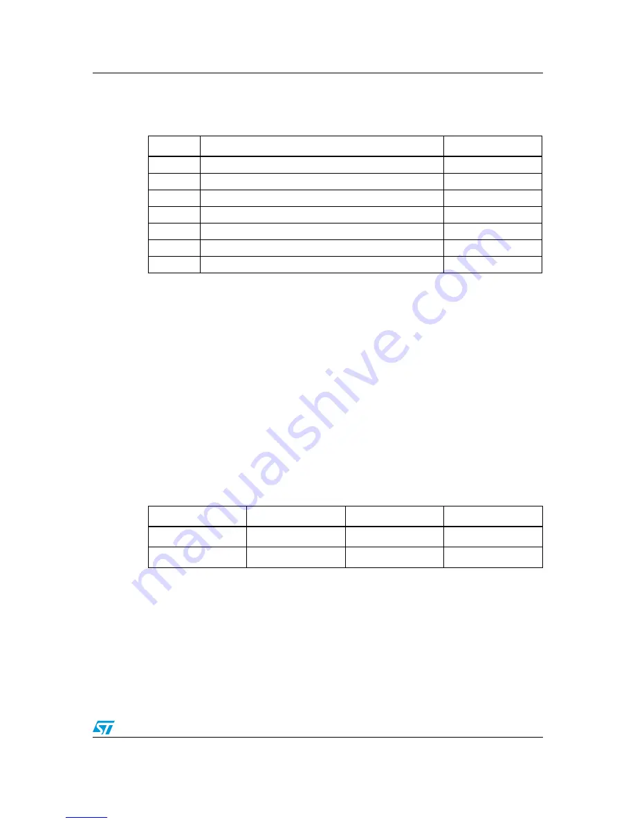
Table 9.
MII/RMII interface selection by solder bridges SB1, SB2 and SB3
SB1
SB2
SB3
MII
Remove
Remove
Fit
RMII
Fit
Fit
Remove
electronic components distributor