SpinCore Technologies PulseBlaster DDS-III Скачать руководство пользователя страница 23

PulseBlasterDDS

* Once the board has been programmed, this step is optional.  If you are just restarting the pulse program

after a STOP command or an HARDWARE_RESET has stopped the program, you can skip this step

during re-initialization.

If these five commands are not sent from a PC, the PulseBlasterDDS will not run as desired.  All five

instructions are required as an attempt to ensure that the device has been programmed before it can be

armed.  The first time the system is used, the loading of the memory with data has to be performed.  Upon

reset, four instructions must be executed to restart the device again.  
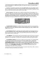
WE for Peripherals: 

This register is used to select the peripheral that is to be programmed.  The

value of this register that is used to select program memory is always zero and this is the default value for

the register.  A complete listing of the values and the associated hardware that can be programmed when

appropriately set is listed below in Table A1.1.  By selecting 0xFF for this value, no device is selected and

the initial value of the output flags may be set.  (*Note that the clock signal to the FF must still be

transitioned, which may be accomplished by writing to the base output port + 5 twice in succession.)

WE Register

Value (hex)

Program Memory

0

Program Frequency Registers

1

Program Phase Registers

2

Change Flags Only

FF

Table A1.1: 

Peripheral List

CLEAR ADDRESS COUNTER:

 The Address Counter is used to manufacture the memory address.

The Address Counter is not loadable; it can only be cleared and started at zero.  It is not possible to load a

particular section of memory.  All loads must start from either the beginning of memory, or wherever the

Address Counter left off.

Flag Initialization Strobe: 

The output flags of the PulseBlasterDDS can be programmed while the

device is in a reset state.  This is useful to initialize flags after powering-up and to reset flags to a known

state if a program must be aborted.  Writing to the Flag Initialization Strobe register will toggle the line

used to clock data into the output latches.

LOAD_MEMORY:

 This instruction is used to specify data that should be used to program the memory

used by the device.  Since the incoming data is taken only one byte at a time, the IBC must reconstruct

the data word to be programmed.  The data word is reconstructed in the IBC most significant byte first.

PROGRAMMING FINISHED:

 This instruction enables the pattern generator of the PulseBlasterDDS.

This instruction prevents the pattern generator from accepting a hardware trigger or software start

command before the device has been programmed.  Once the design has been programmed, the

PROGRAMMING FINISIHED

 command must be sent to arm the device for operation.  After the pattern

generator has been armed, any hardware trigger or software start command will cause the system to start
operation. The PulseBlasterDDS can be reset by issuing the 

DEVICE_RESET

 command.  This will

internally clear the 

PROGRAMMING FINISHED

 instruction and prevent the pattern generator from

operating again until the IBC has been re-initialized.

In order to select each of the commands mentioned about, you write to the port base + offset.  A table of

each offset’s meaning is included below, see next page.

9/20/200523

www.spincore.com

Содержание PulseBlaster DDS-III

Страница 1: ...PulseBlasterDDS Model DDS III PCI Board SP3 Owner s Manual SpinCore Technologies Inc http www spincore com...

Страница 2: ...nologies Inc reserves the right to make changes to the product s or information herein without notice PulseBlasterDDS PulseBlaster SpinCore and the SpinCore Technologies Inc logos are trademarks of Sp...

Страница 3: ...ions 8 Pulse Program Control Flow Common 8 II Installation 9 Installing the PulseBlasterDDS Driver 9 For Windows XP 9 Initializing Control of the PulseBlasterDDS 10 III Programming the PulseBlasterDDS...

Страница 4: ...Connector labeled SMA400 18 Appendix I Sample C program 19 Example Program 19 Appendix II Programming the PulseBlasterDDS Using Direct Outputs 22 Using DLL Functions to Send Instructions 22 Building...

Страница 5: ...tem control and pulse synchronization By adding DDS features PulseBlasterDDS can now provide not only digital TTL but also analog output signals meeting high performance and high precision complex exc...

Страница 6: ...se and functions as a phase reset for the DDS generator The frequency and phase of the RF pulses generated by the DDS are under the control of the user and are specified through software programming T...

Страница 7: ...t Instruction set PulseBlasterDDS design features a set of commands for highly flexible program flow control The micro programmed controller allows for programs to include branches subroutines and loo...

Страница 8: ...ns 10 individually controlled digital output lines TTL levels one of the output lines has a dual use and functions as a phase reset for the DDS generator variable pulses delays for every TTL line 25 m...

Страница 9: ...computer 4 Insert the PulseBlasterDDS board into an empty PCI slot Secure the bracket firmly with a screw 5 Turn on your computer For Windows XP 6 After booting the Found New Hardware Wizard should a...

Страница 10: ...ttp www pulseblaster com CD PulseBlasterDDS PCI SP3 old_version post_installation_files zip in order for your board to work You are now ready to control the PulseBlasterDDS board Initializing Control...

Страница 11: ...ve clock cycles for 512 memory word models and the longest being 2 52 clock cycles All instructions have the same format and bit length and all bit fields have to be filled Figure 3 shows the fields a...

Страница 12: ...Field and Op Code Please refer to Table 2 for information on the available operational codes OpCode and the associated data field functions the data field s function is dependent on the Op Code Op Co...

Страница 13: ...device Used to initialize the system to receive programming information It accepts a parameter referencing the target for the instructions Valid values for device are PULSE_PROGRAM FREQ_REGS PHASE_RE...

Страница 14: ...s are 0x0 to 0x3FF For example 0x010 would correspond to bit 5 being on and all other bits being off Bit 10 corresponding to hexadecimal value 0x200 is used to reset the phase of the numerically contr...

Страница 15: ...perates at 100MHz set_clock 100 Prepare the Board to Receive Freqeuncy Values start_programming FREQ_REGS Load Frequency Register 0 set_freq 1 054 Load Frequency Register 1 set_freq 2 Prepare the Boar...

Страница 16: ...tput ON Phase Reg 0 for DAC_OUT_0 and DAC_OUT_2 DDS RX Output ON Flags 0x000 OPCODE BRANCH pb_inst 0 1 TX_ANALOG_ON 0 RX_ANALOG_ON 0x000 BRANCH start 2 us Finished Sending Instructions stop_programmin...

Страница 17: ...ctor Figure 4 SMA Connectors DB 25 TTL Output Signal Bits Outputs TTL signals generated by the user s Program Please consult the table below for bit assignments Pin Assignments Pin Bit Pin Bit 1 GND 1...

Страница 18: ...ult and pin 1 is active pin 2 GND When a low state is detected e g when shorting pins 1 2 it initiates code execution This trigger will also restart execution of a program from the beginning of the co...

Страница 19: ...program Example Program Example2 cpp SpinCore Technologies Inc May 2004 http www spincore com The following program code uses C Functions from pbdfuncts to generate and execute a pulse sequence on th...

Страница 20: ...set_phase 135 Set register 6 set_phase 157 5 Set register 7 set_phase 180 Set register 8 set_phase 202 5 Set register 9 set_phase 225 Set register 10 set_phase 247 5 Set register 11 set_phase 270 Set...

Страница 21: ...instruction in 1us pb_inst 0 0 TX_ANALOG_ON 0 RX_ANALOG_OFF 0x0 END_LOOP loop 1 us Instruction 3 Stay here for 5 1us then continue to Instruction 4 pb_inst 0 0 TX_ANALOG_OFF 0 RX_ANALOG_ON 0x0 LONG_D...

Страница 22: ...erDDS PCI board It returns a 0 upon successful completion or a negative number for an error Building Instructions Using the DLL Functions To send instructions to the PulseBlasterDDS the programmer mus...

Страница 23: ...d at zero It is not possible to load a particular section of memory All loads must start from either the beginning of memory or wherever the Address Counter left off Flag Initialization Strobe The out...

Страница 24: ...address counter Set initial flag values Values for this example are 0x000000f0 PBD03PC_outp 6 0 Data transfer PBD03PC_outp 6 0 Data transfer PBD03PC_outp 6 0 Data transfer PBD03PC_outp 6 0xF0 Data tr...

Страница 25: ...C_outp 6 0x00 Data Transfer Byte 1 of Reg1 PBD03PC_outp 6 0x00 Data Transfer Byte 0 of Reg1 PBD03PC_outp 6 0xE0 Data Transfer Byte 3 of Reg15 PBD03PC_outp 6 0x00 Data Transfer Byte 2 of Reg15 PBD03PC_...

Страница 26: ...PulseBlasterDDS Only execute the following command when you are ready for the program to start running PBD03PC_outp 1 0 Start pulse program 9 20 200526 www spincore com...

Страница 27: ...sterDDS Contact Information Phone 352 271 7383 FAX 352 371 8679 Email sales spincore com Web http www spincore com Product URL http www pulseblaster com CD PulseBlasterDDS PCI SP3 9 20 200527 www spin...

Отзывы: