


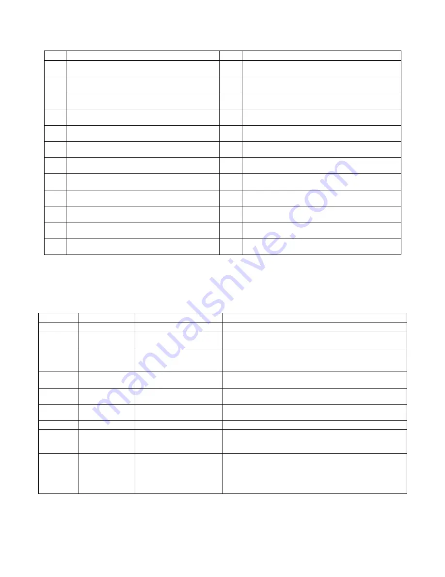
PulseBlasterDDS
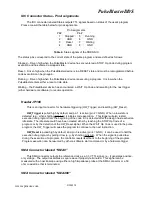
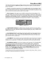
Bit #
Function
Bit #
Function
23
Selects Frequency Register (bit 3)
11
Selects Phase Register for SMA connectors
labeled DAC_OUT_2 and DAC_OUT_0 (bit 0)
22
Selects Frequency Register (bit 2)
10
Output Enable for SMA connectors labeled
DAC_OUT_1 and DAC_OUT_0 (0 = on, 1 = off)
21
Selects Frequency Register (bit 1)
9
RF phase reset for phase coherent switching,
also routed to Output Connector DB25 pin 19
20
Selects Frequency Register (bit 0)
8
Output Connector DB25 pin 7
19
Selects Phase Register for SMA connector
labeled DAC_OUT_1 (bit 3)
7
Output Connector DB25 pin 8
18
Selects Phase Register for SMA connector
labeled DAC_OUT_1 (bit 2)
6
Output Connector DB25 pin 21
17
Selects Phase Register for SMA connector
labeled DAC_OUT_1 (bit 1)
5
Output Connector DB25 pin 22
16
Selects Phase Register for SMA connector
labeled DAC_OUT_1 (bit 0)
4
Output Connector DB25 pin 10
15
Output Enable for SMA connector labeled
DAC_OUT_2 (0 = on, 1 = off)
3
Output Connector DB25 pin 11
14
Selects Phase Register for SMA connectors
labeled DAC_OUT_2 and DAC_OUT_0 (bit 3)
2
Output Connector DB25 pin 24
13
Selects Phase Register for SMA connectors
labeled DAC_OUT_2 and DAC_OUT_0 (bit 2)
1
Output Connector DB25 pin 25
12
Selects Phase Register for SMA connectors
labeled DAC_OUT_2 and DAC_OUT_0 (bit 1)
0
Output Connector DB25 pin 13
Table 1:
Output Pattern and Control Word Bits
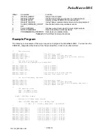
Data Field and Op Code
Please refer to Table 2 for information on the available operational codes (OpCode) and the
associated data field functions (the data field's function is dependent on the Op Code)
Op Code Instruction
Data Field
Function
0
CONTINUE
Ignored
Program execution continues to next instruction
1
STOP
Ignored
Stop execution of program (*Note all TTL values remain
from previous instruction, and analog outputs turn off)
2
LOOP
Number of desired loops.
This value must be greater
than or equal to 1.
Specify beginning of a loop. Execution continues to next
instruction. Data used to specify number of loops
3
END_LOOP
Address of beginning of
loop
Specify end of a loop. Execution returns to begging of
loop and decrements loop counter.
4
JSR
Address of first subroutine
instruction
Program execution jumps to beginning of a subroutine
5
RTS
Ignored
Program execution returns to instruction after JSR was
called
6
BRANCH
Address of next instruction
Program execution continues at specified instruction
7
LONG_DELAY
Number of desired loops.
This value must be greater
than or equal to 2.
For long interval instructions. Data field specifies a
multiplier of the delay field. Execution continues to next
instruction
8
WAIT
Ignored
Program execution stops and waits for software or
hardware trigger. Execution continues to next instruction
after receipt of trigger. The latency is equal to the delay
value entered in the WAIT instruction line plus a fixed
delay of 6 clock cycles.
Table 2:
Op Code and Data Field Description
Delay Count
9/20/200512
www.spincore.com


