SOYO 5TS0 Скачать руководство пользователя страница 26

20

Hardware Setup

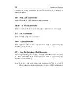
J6, U22 – Universal Serial Bus Connector (Optional)

Attach USB cable to these connectors for external USB device.

MPEG Connector – MPEG Daughter Board Connector
(Optional)

You could attach H/W MPEG Daughter Board to perform the H/W
MPEG function.  Due to the various design, contact your dealer for the
H/W MPEG function.

TT Connector – TV Tuner/Feature Connector (Optional)

Attach TV Tuner/Feature Connector cable to this connector to enable the
TV Tuner/Feature Connector function.

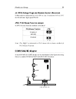
Line Out – Line Out Connector

Linking one end of the line out cable to this connector and the other end
to COM/VGA/LINE adapter to enable line out function.

Line Out Cable

If you have S3 MPEG Daughter Board attached, you will need a Line
Out Cable to enable the Line Out function.  Please contact the M/B
manufacture for the Line Out cable.)

IR – Infra Red Connector (Optional)

Attach Infra Red device cable to this connector to enable the infrared
transfer function.

Содержание 5TS0

Страница 1: ...Pentium 82430 HX P54C PCI Mainboard User s Guide Technical Reference 5TS0 S2 S5...

Страница 2: ...the specifications of the product described within it at any time without notice and without obligation to notify any person of such revision or change The information contained in this manual is pro...

Страница 3: ...rs 7 Factory Set Jumpers 7 JP3 Display Type 7 JP10 Sleep Switch Connector Enable Disable 7 JP32 JP33 Bus Fraction Core Bus Ratio Select 8 JP5 CMOS Clear Jumper 8 J4 VRM Voltage Regulator Module Socket...

Страница 4: ...18 J2 PS 2 Mouse Connector 19 J22 Turbo LED Connector 19 IDE1 IDE2 On board Primary Secondary IDE HDD Connectors 19 J11 HDD LED Connectors 19 COM VGA LINE Connectors 19 FDC1 Connector 19 P1 Parallel P...

Страница 5: ...33 Supervisor Password 35 User Password 36 IDE HDD Auto Detection 37 Chapter 4 Drivers Installation Guide 38 IDE BUS Master Installation Guide 38 MS DOS WINDOW WFW 38 WINDOWS NT3 5 38 WINDOWS 95 39 NO...

Страница 6: ......

Страница 7: ...ode both symmetrical and asymmetrical addressing and EDO DRAM 72 pin SIMM On board memory configurations from 4 to 256 Mbytes Supports Error Checking and Correction ECC and Parity Check Optional On bo...

Страница 8: ...sted video playback up to 1024x768x16 bits pixel Support for India Cinepak and software accelerated MPEG 1 video playback S3 Scenic Highway Interface H W MPEG Philips SAA7110 SAA7111 video digitizers...

Страница 9: ...Bs DRAM 640x480x16 640x480x256 640x480x64K 800x600x16 800x600x256 800x600x64K 1024x768x16 1024x768x256 1024x768x64K 1152x864x256 1280x1024x16 1280x1024x256 1600x1200x16 IL 1600x1200x256 IL Note IL mea...

Страница 10: ...f there is damage to the board contact your dealer immediately Electrostatic Discharge Precautions Make sure you ground yourself before handling the mainboard or other system components Electrostatic...

Страница 11: ...AM 13 IDE1 IDE2 Connector 3 82430 HX Chipset 14 Floppy Connector 4 Pipelined Burst SRAM Module Slot 15 Parallel Port Connector 5 PnP FLASH BIOS 16 COM1 COM2 VGA LINE Connector 6 Real Time Clock RTC 17...

Страница 12: ...S2 JP3 Super I O CHIP DRAM BANK PCI SLOT IDE1 IDE2 ISA SLOT 16Kx8 TAG 16Kx8 TAG P B SRAM 32k x 32 P B SRAM 32k x 32 Pipelined Burst SRAM Module Slot FLASH BIOS FDC1 P1 PW1 J1 J2 1 1 Super I O CHIP JP2...

Страница 13: ...e performing any work on the mainboard or system Jumpers Factory Set Jumpers The following jumpers are set at the factory as below Jumpers Factory settings JP1 JP14 JP15 JP34 Factory fixed at 2 3 JP2...

Страница 14: ...tium 75 90 100MHz AMD 5k86 SSA5 P75 P90 P100MHz AMD 5k86 K5 P120 P133MHz JP32 JP33 2 1 Pentium 120 133MHz Cyrix P120 P133 P150 P166 MHz AMD 5k86 K5 P150 P166MHz JP32 JP33 5 2 Pentium 150 166MHz JP32 J...

Страница 15: ...tion Jumper Set PS 2 mouse function enabled or disabled PS 2 Mouse Function JPS2 Disabled default 1 2 Enabled 1 2 Note The IRQ12 is dedicated to PS 2 mouse when choose enabled of PS 2 Mouse Function C...

Страница 16: ...onnector Attach COM1 cable to this connector JP2 COM2 Connector Attach COM2 cable to this connector this cable is provided by the mainboard manufacture J2 Line Out Mainboard End Connector Attach 4 pin...

Страница 17: ...ings 1 5 x clock 586 CPU Family Pipelined Burst SRAM Module Slot JP12 JP13 JP32 JP33 Pentium P54CX 75 50 MHz AMD K5 SSA5 PR75 50 MHz Red Caps JP12 JP13 Pentium P54CX 90 60 MHz AMD K5 SSA5 PR90 60 MHz...

Страница 18: ...m P54CX 100 50 MHz Cyrix 6x86 P120 50 MHz Red Caps JP12 JP13 Pentium P54CX 120 60 MHz Cyrix 6x86 P150 60 MHz AMD K5 PR150 60 MHz Red Caps JP12 JP13 Cyrix 6x86 P133 55 MHz Red Caps JP12 JP13 Pentium P5...

Страница 19: ...Figure 2 1 3 CPU Jumper Settings Note You must equip the CPU with a fan and heat sink for system stability Pentium 180 200 CPU Settings 3 0 x clock 586 CPU Family Pipelined Burst SRAM Module Slot JP12...

Страница 20: ...86 Refer to the following figure to set these CPUs voltage JP27 JP30 586 CPU Family Pipelined Burst SRAM Module Slot JP24 JP26 JP29 JP36 1 4 JP27 JP30 3 3V CPU JP27 JP30 3 45V 3 6V CPU Figure 2 2 1 Si...

Страница 21: ...rity The mainboard requires SIMM of at least 70ns access time Single side SIMM Double side SIMM 4MB 1MB x 36 32 2MB 512K x 36 32 16MB 4MB x 36 32 8MB 2MB x 36 32 64MB 16MB x 36 32 32MB 8MB x 36 32 The...

Страница 22: ...e Size Cache RAM TAG RAM Cacheable Range 256KB 32K x32 2 pcs or 256K module on U31 U32 or J3 16K x 8 on U27 U28 512 MB Upgrade to 512KB 32K x 32 2pcs 256K module on U31 U32 and J3 16K x 8 on U27 U28 5...

Страница 23: ...Burst SRAM Module Slot JP31 Figure 2 3 2 512K Pipelined Burst Cache Configuration Multi I O Port Addresses Default settings for multi I O port addresses are shown in the table below Port I O Address...

Страница 24: ...at least 200 watts and a power good signal PW1 has two six pin male header connectors Plug the dual connectors from the power directly onto the board connector while making sure the black leads are i...

Страница 25: ...ttach on board hard disk drive LEDs to this connector The LED lights when an HDD is active COM VGA LINE Connectors Attach COM1 COM2 VGA LINE OUT adapter to these connectors FDC1 Connector Attach flopp...

Страница 26: ...ional Attach TV Tuner Feature Connector cable to this connector to enable the TV Tuner Feature Connector function Line Out Line Out Connector Linking one end of the line out cable to this connector an...

Страница 27: ...RD I O SETUP LOAD SETUP DEFAULTS LOAD BIOS DEFAULTS INTEGRATED PERIPHERALS SUPERVISOR PASSWORD USER PASSWORD IDE HDD AUTO DETECTION SAVE EXIT SETUP EXIT WITHOUT SAVING Time Date Hard Disk Type Esc Qui...

Страница 28: ...1 Help Shift F2 Change Color F3 Toggle Calendar Base Memory 640K Extended Memory 3328K Other Memory 128K Total Memory 4096K 2 Use arrow keys to move between items and select values Modify selected fie...

Страница 29: ...Defaults Video BIOS Shadow Enabled C8000 CBFFF Shadow Disabled CC000 CFFFF Shadow Disabled D0000 D3FFF Shadow Disabled D4000 D7FFF Shadow Disabled D8000 DBFFF Shadow Disabled DC000 DFFFF Shadow Disab...

Страница 30: ...1MB using the fast gate A20 line Typematic Rate Setting Enable this option to adjust the keystroke repeat rate Typematic Rate Chars Sec Choose the rate a character keeps repeating Typematic Delay Msec...

Страница 31: ...Adapter BIOS Shadow BIOS shadow copies BIOS code from slower ROM to faster RAM BIOS can then execute from RAM These 16K segments can be shadowed from ROM to RAM BIOS is shadowed in a 16K segment if i...

Страница 32: ...tion Enabled DRAM Timing 70 ns DRAM RAS Precharge Time 4 DRAM R W Leadoff Timing 7 6 Fast RAS To CAS Delay 3 DRAM Read Burst Timing x333 x444 DRAM Write Burts Timing x333 Turbo Read Leadoff Disabled D...

Страница 33: ...ead Burst Timing Use the default setting DRAM Write Burst Timing Use the default setting Turbo Read Leadoff Use the default setting DRAM Speculative Leadoff Use the default setting Turn Around Inserti...

Страница 34: ...herwise use Disabled Peer Concurrency Use the default setting Chipset Special Features Use the default setting DRAM ECC PARITY Select Choose ECC or Parity default according the type of DRAM you have M...

Страница 35: ...Modify F5 Old Values Shift F2 Color F6 Load BIOS Defaults F7 Load Setup Defaults Power Down Resume Events IRQ 3 COM 2 ON IRQ 4 COM 1 ON IRQ 5 LPT 2 ON IRQ 6 Floppy Disk OFF IRQ 7 LPT 1 ON IRQ 8 RTC Al...

Страница 36: ...his mode Time is adjustable from 1 Min to 1 Hour Under Suspend mode the CPU stops completely no instructions are executed HDD Power Down When the set time has elapsed the BIOS sends a command to the H...

Страница 37: ...gacy ISA DMA 0 assigned to PCI ISA PnP DMA 1 assigned to PCI ISA PnP DMA 3 assigned to PCI ISA PnP DMA 5 assigned to PCI ISA PnP DMA 6 assigned to PCI ISA PnP DMA 7 assigned to PCI ISA PnP PCI IRQ Act...

Страница 38: ...IDE is inserted The default setting is PCI AUTO If PCI AUTO does not work then assign an individual PCI SLOT number Primary IDE INT Choose INTA INTB INTC or INTD The default setting is INTA Secondary...

Страница 39: ...ain Menu and the following screen appears The screen below shows default settings ROM PCI ISA BIOS INTEGRATED PERIPHERALS AWARD SOFTWARE INC ESC Quit Select Item F1 Help PU PD Modify F5 Old Values Shi...

Страница 40: ...ary Master PIO IDE Primary Slave PIO IDE Secondary Master PIO IDE Secondary Slave PIO Choose Auto default or mode 0 4 Mode 0 is the slowest speed and HDD mode 4 is the fastest speed For better perform...

Страница 41: ...oard Printer Mode Choose ECP EPP default SPP or EPP ECP mode The mode depends on your external device that connects to this port ECP Mode DMA Select Choose DMA3 default or DMA1 This setting only works...

Страница 42: ...word 2 Enter a password and press Enter If you do not wish to use the password function you can just press Enter and a Password disabled message appears 3 After you enter your password the following m...

Страница 43: ...password and press Enter If you do not wish to use the password function you can just press Enter and a Password disabled message appears 3 After you enter your password the following message appears...

Страница 44: ...UP accordingly Note This function is only valid for IDE hard disks ROM PCI ISA BIOS CMOS SETUP UTILITY AWARD SOFTWARE INC Do you accept this drive C Y N N ESC Skip HARD DISKS TYPE SIZE CYLS HEAD PRECO...

Страница 45: ...r Option dialog will appear select Other Requires a disk from a hardware manufacturer from the Adapter list box 5 Next the Insert Diskette dialog box will appear insert the Triones PIIX PIIX3 Bus Mast...

Страница 46: ...n the system console and on the command prompt state type in load TRIN4X DSK Enter or load TRIN312 DSK Enter You can also include the above command line into the start up file STARTUP NCF to load the...

Страница 47: ...rfd0135ds9 3 5 DSDD Now you have already made an installation diskette for the device driver Start the installation by typing custom 6 Select the Install operation and then follow the guided steps Wh...

Страница 48: ...ver by typing install 6 Reboot your SCO UNIX system OS 2 2 0 and WARP 3 X 1 Copy TRIOS2 ADD from the floppy diskette to your hard disk under the OS2 directory i e C OS2 2 Edit C CONFIG SYS to replace...

Отзывы: