


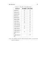


Introduction
5
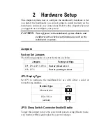
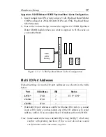
Mainboard Layout w/ Default Settings
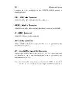
1
13
9
7
10
11
12
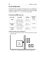
18
17
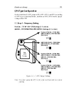
2
3
5
6
8
3
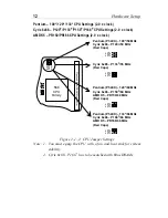
14
16
4
18
2
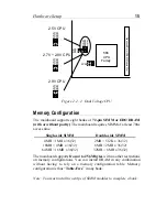
19
20
20
20
20
21
15
21
21
22
Figure 1Ð1. Mainboard Layout
1.
P54C/6x86 in ZIF socket 7
12.
PS/2 Mouse Connector
2.
Pipelined Burst SRAM
13.
IDE1/IDE2 Connector
3.
82430 HX Chipset
14.
Floppy Connector
4.
Pipelined Burst SRAM Module
Slot
15.
Parallel Port Connector
5.
PnP FLASH BIOS
16.
COM1/COM2/VGA/LINE
Connector
6.
Real Time Clock (RTC)
17.
Keyboard BIOS
7.
ISA Slots
18.
Super I/O Chipset
8.
PCI Slots
19.
S3 VGA Chips
9.
SIMM Memory Bank
20.
EDO DRAM (for Video)
10.
5V DC Power Connector
21.
MPEG Connector (Optional)
11.
Keyboard Connector
22.
TV Tuner/Feature Connector
(Optional)
Содержание 5TS0
Страница 1: ...Pentium 82430 HX P54C PCI Mainboard User s Guide Technical Reference 5TS0 S2 S5...
Страница 6: ......