


4-2
WRU-806B
4-2. CPU Pin Description
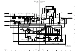
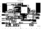
4-2-1. Pin Description of CPU (IC601 on RF-155 Board)
Pin No.
Pin name
I/O
Description
1
Avcc
_
_
2
MS_DATA_IN
I
It becomes the value of the data communication line
(receiver) during Master/Subordinate (sub) and a reversed value.
3
MS_DATA_OUT
O
It becomes the value of the data communication line (transmitter) during
Master/Subordinate (sub) and a reversed value.
4
WRU/URX
I
Model selection terminal
High: WRU / Low: URX
5
TEST
I
Tx/Rx selection terminal
.
High: Tx (Operate as a transmitter)
.
Low: Rx (Operate as a receiver)
6
DBG
I/O
Input-output terminal for debugging
7
TXD
O
Pull-up
Transmission terminal for RS232C communication
8
RXD
I
Pull-up
Reception terminal for RS232C communication
9
KEY_GP
I
“Gp” key input terminal
.
Low: Key on
.
High: Key off
10
KEY_CH
I
“CH” key input terminal
.
Low: Key on
.
High: Key off
11
KEY_PLUS
I
“
+
” key input terminal
.
Low: Key on
.
High: Key off
12
KEY_MINUS
I
“
_
” key input terminal
.
Low: Key on
.
High: Key off
13
EEP_SDA
I
Data terminal of IIC communication for EEPROM
14
EEP_SCL
O
Clock terminal of IIC communication for EEPROM
15
EEP_WP
O
Write protection terminal of IIC communication for EEPROM
.
High: Impossible
.
Low: Possible
16
NC
O
Not used
17
NC
O
Not used
18
X0
_
_
19
X1
_
_
20
Vss
_
Vss
21
Vcc
_
Vcc
22
NC
O
Not used
23
X1A
O
Not used
24
X0A
O
Not used
25
/RST
I
_
26, 27
V3
I
LCD bias
27
V2
I
LCD bias
28
V1
I
LCD bias
29
V0
I
LCD bias
30
NC
O
Not used