
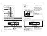


1-4
WRR-802A (U)
11
US
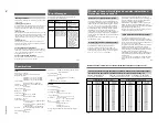
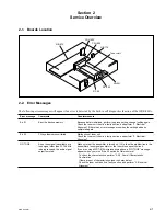
Apart from the normal indications, the following error
messages may appear on the display.
Meaning
Remedy
Err 01
Message
An error has occurred in
the backup memory data.
The memory data is
initialized. Reset the
group and channel
settings.
Contact your nearest
Sony dealer.
The PLL-synthesized
circuit has a malfunction.
Err 02
NO TONE
As no tone signal is
available or a tone signal
other than 32.768 kHz is
being received, the audio
signal output is muted.
Make sure that the
transmitter is turned on.
If it is, then the problem
lies in the transmitter’s
tone signal generator or
the tuner’s tone squelch
circuit. Contact your
nearest Sony dealer.
If you are using a WRT-
810A wireless
microphone, a “NO
TONE” message
appears when you turn
off the AF switch, but
this is normal.
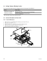
Error Messages
Muting Functions
This unit has the following three muting functions, which work
in combination.
(1) Muting by RF input level
As sufficient S/N for the audio output may not be obtained if no
RF signal is received or the RF input level is low, the audio
output can be muted when the RF input level falls below the
muting level.
(2) Tone squelch
The audio output is obtained only when the unit receives an RF
signal which includes a specified tone signal. The audio output
is muted to eliminate noise which may be heard when the
transmitter is turned on/off or the unit receives an interference
RF signal.
(3) Noise squelch
The audio output is muted to eliminate noise which may be
heard when there is such excessive interference RF signal that
the tone squelch does not work.
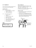
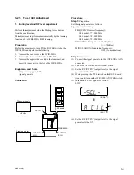
To turn off the muting functions
While holding down the GP and CH buttons, turn the POWER
switch to ON. All indications momentarily appear, then go off.
“OFF” is then displayed. This procedure cancels all three
muting functions at the same time.
To turn on the muting functions
Turn the POWER switch to OFF, then to ON again. The three
muting functions are activated at the same time.
12
US
Tuner
Reception type 110KF3E
Circuit system Dual conversion superheterodyne
Reception frequencies
U64 model: 770.125 to 781.875 MHz
U66 model: 782.125 to 793.875 MHz
U68 model: 794.125 to 805.875 MHz
Local oscillators
Crystal controlled PLL synthesizer
Selectivity
60 dB or more (at ±250 kHz detuned)
Spurious rejection ratio
70 dB or more
Image rejection ratio
60 dB or more
Muting level
30 dBµ
1)
Antenna connectors
BNC-R type (2), 50 ohms
Frequency response
100 to 15,000 Hz ±3 dB
De-emphasis
50 µsec
Signal-to-noise ratio
40 dB or more at an A-weighted RF input
level of 20 dBµ
60 dB or more at an A-weighted RF input
level of 60 dBµ
(±5 kHz deviation at 1 kHz modulation)
Distortion
1% or less (±40 kHz deviation at 1 kHz
modulation)
Tone signal frequency
32.768 kHz
Specifications
Output level
–20 dBm
2)
or –58 dBm (±5 kHz deviation at
1 kHz modulation)
Output impedance
150 ohms
Output connector
ø6.3 phone balanced (
1
/
4
inch TRS)
XLR-3-12C
1) 0 dBµ=1 µV
2) 0 dBm=0.775 Vrms (600 ohms loaded)
General
Power requirements
9 V DC
Current consumption
Approx. 600 mA
Operating temperature
0°C to 40°C (32°F to 104°F)
Storage temperature
–20°C to +55°C (–4°F to +131°F)
Dimensions
218
×
44
×
210 mm
(8
5
/
8
×
1
3
/
4
×
8
3
/
8
inches) (w/h/d)
Mass
Approx. 1.6 kg (3 lb 8 oz)
Accessories supplied
AC power adaptor (1)
Antennas (2)
Operating Instructions (1)
Design and specifications are subject to change without
notice.
L-1
Guidance on use of multi-channel system
This product is designed to give excellent interference free
operation in multi-channel systems. To maintain this, Sony
recommends that one of the original Sony groups, number
00, 11, 12, 13, A1, A2, A3, L1, L2, H1 or H2 is selected.
These groups will offer excellent performance, free from
mutual interference from other Sony wireless microphone
transmitters in the selected group when used under the
recommended operating conditions. The remaining groups
are included for compliance with frequency regulations in
various countries, and will not always guarantee interference
free operation.
Group 00 is used to scan for open channels, or to use only
for a one channel system.
Directrices para el uso de sistemas multicanal
Este producto se ha diseñado para proporcionar una
operación excelente sin interferencias en sistemas de
múltiples canales. Para esto, Sony recomienda seleccionar
uno de los grupos originales de Sony, es decir, los número
00, 11, 12, 13, A1, A2, A3, L1, L2, H1 o H2.
Estos grupos ofrecen un funcionamiento excelente, sin
interferencias en ambos sentidos con otros transmisores de
micrófono inalámbrico de Sony del grupo seleccionado,
siempre que se utilicen en las condiciones de
funcionamiento recomendadas. Los demás grupos se han
incluido por motivos de compatibilidad con las normas
sobre frecuencias de varios países y no siempre garantizarán
un funcionamiento sin interferencias.
El grupo 00 sirve para buscar canales abiertos o se utiliza
solamente para sistemas de un solo canal.
Guide d’utilisation du système multicanal
Ce produit est conçu pour assurer un excellent
fonctionnement exempt d’interférences dans les systèmes
multicanaux. A cette fin, Sony recommande de sélectionner
l’un des groupes Sony originaux portant les numéros 00, 11,
12, 13, A1, A2, A3, L1, L2, H1 et H2.
Ces groupes offrent d’excellentes performances, exemptes
d’interférences mutuelles avec d’autres emetteurs de
microphone sans fil Sony dans le groupe sélectionné s’ils
sont exploités dans les conditions d’utilisation préconisées.
Les autres groupes sont inclus pour satisfaire aux
réglementations sur les fréquences dans les différents pays
et ne garantissent pas toujours un fonctionnement exempt
d’interférences.
C’est le groupe 00 qui est utlilisé pour explorer les canaux
ouverts, ou en vue de l’utilisation d’un système à canal
unique.
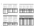
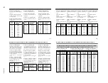
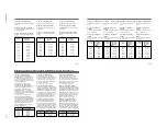
Wireless Channel Lists/Listas de canales inalámbricos/
Listes des canaux sans fil
L-2
Wireless Channel Lists/Listas de canales inalámbricos/Listes des canaux sans fil
For 68-Version Model Using TV Channels 68 and 69/Para modelos de la versión 68 que utilizan
los canales de TV 68 y 69/Pour le modèle 68 utilisant les canaux de télévision 68 et 69
Group 00: All channel access
Use to scan for open channels.
Groupe 00: Accès tous canaux
Pour l’exploration des canaux ouverts.
Grupo 00: Acceso a todos los canales
Se utiliza para buscar canales abiertos.
Channel
Canal
Frequency (MHz)
Frequencia
Fréquence
Channel
Canal
Frequency (MHz)
Frequencia
Fréquence
Channel
Canal
Frequency (MHz)
Frequencia
Fréquence
Channel
Canal
Frequency (MHz)
Frequencia
Fréquence
TV-68 Band/Banda de TV 68/Bande télé 68
TV-69 Band/Banda de TV 69/Bande télé 69
68-01
794.125
68-25
797.125
68-02
794.250
68-26
797.250
68-03
794.375
68-27
797.375
68-04
794.500
68-28
797.500
68-05
794.625
68-29
797.625
68-06
794.750
68-30
797.750
68-07
794.875
68-31
797.875
68-08
795.000
68-32
798.000
68-09
795.125
68-33
798.125
68-10
795.250
68-34
798.250
68-11
795.375
68-35
798.375
68-12
795.500
68-36
798.500
68-13
795.625
68-37
798.625
68-14
795.750
68-38
798.750
68-15
795.875
68-39
798.875
68-16
796.000
68-40
799.000
68-17
796.125
68-41
799.125
68-18
796.250
68-42
799.250
68-19
796.375
68-43
799.375
68-20
796.500
68-44
799.500
68-21
796.625
68-45
799.625
68-22
796.750
68-46
799.750
68-23
796.875
68-47
799.875
68-24
797.000
69-01
800.125
69-25
803.125
69-02
800.250
69-26
803.250
69-03
800.375
69-27
803.375
69-04
800.500
69-28
803.500
69-05
800.625
69-29
803.625
69-06
800.750
69-30
803.750
69-07
800.875
69-31
803.875
69-08
801.000
69-32
804.000
69-09
801.125
69-33
804.125
69-10
801.250
69-34
804.250
69-11
801.375
69-35
804.375
69-12
801.500
69-36
804.500
69-13
801.625
69-37
804.625
69-14
801.750
69-38
804.750
69-15
801.875
69-39
804.875
69-16
802.000
69-40
805.000
69-17
802.125
69-41
805.125
69-18
802.250
69-42
805.250
69-19
802.375
69-43
805.375
69-20
802.500
69-44
805.500
69-21
802.625
69-45
805.625
69-22
802.750
69-46
805.750
69-23
802.875
69-47
805.875
69-24
803.000