REF. NO.
PART NO.
DESCRIPTION
REMARK
------------
-------------
-------------------
-------------
REF. NO.
PART NO.
DESCRIPTION
REMARK
------------
-------------
-------------------
-------------
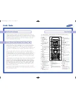
The components identified by
shading and mark
!
are criti-
cal for safety.
Replace only with part number
specified.
– 113 –
-------------------------------------------------------------------------------------------------------------------------------
-------------------------------------------------------------------------------------------------------------------------------
-------------------
C418
1-130-488-00
MYLAR\T0.027MF 5%
50V
C418
1-130-488-00
MYLAR\T0.027MF 5%
50V
C419
1-124-257-00
ELECT\T2.2MF
20%
50V
C419
1-124-257-00
ELECT\T2.2MF
20%
50V
C421
1-104-665-11
ELECT\T100MF
20%
10V
C421
1-104-665-11
ELECT\T100MF
20%
10V
C422
1-163-018-00
CERAMIC CHIP\T0.0056MF
10%
50V
C422
1-163-018-00
CERAMIC CHIP\T0.0056MF
10%
50V
C424
1-126-160-11
ELECT\T1MF
20%
50V
C424
1-126-160-11
ELECT\T1MF
20%
50V
C425
1-163-038-91
CERAMIC CHIP\T0.1MF
25V
C425
1-163-038-91
CERAMIC CHIP\T0.1MF
25V
C430
1-163-227-11
CERAMIC CHIP\T10PF
0.5PF 50V
C430
1-163-227-11
CERAMIC CHIP\T10PF
0.5PF 50V
C431
1-163-231-11
CERAMIC CHIP\T15PF
5%
50V
C431
1-163-231-11
CERAMIC CHIP\T15PF
5%
50V
C432
1-163-038-91
CERAMIC CHIP\T0.1MF
25V
C432
1-163-038-91
CERAMIC CHIP\T0.1MF
25V
C435
1-163-038-91
CERAMIC CHIP\T0.1MF
25V
C435
1-163-038-91
CERAMIC CHIP\T0.1MF
25V
C436
1-104-665-11
ELECT\T100MF
20%
10V
C436
1-104-665-11
ELECT\T100MF
20%
10V
C441
1-163-031-11
CERAMIC CHIP\T0.01MF
50V
C441
1-163-031-11
CERAMIC CHIP\T0.01MF
50V
C455
1-126-924-11
ELECT\T330MF
20%
6.3V
C455
1-126-924-11
ELECT\T330MF
20%
6.3V
C456
1-163-009-11
CERAMIC CHIP\T0.001MF
10%
50V
C456
1-163-009-11
CERAMIC CHIP\T0.001MF
10%
50V
C457
1-163-009-11
CERAMIC CHIP\T0.001MF
10%
50V
C457
1-163-009-11
CERAMIC CHIP\T0.001MF
10%
50V
C458
1-163-009-11
CERAMIC CHIP\T0.001MF
10%
50V
C458
1-163-009-11
CERAMIC CHIP\T0.001MF
10%
50V
C460
1-163-009-11
CERAMIC CHIP\T0.001MF
10%
50V
C460
1-163-009-11
CERAMIC CHIP\T0.001MF
10%
50V
C701
1-163-033-91
CERAMIC CHIP\T0.022MF
50V
C701
1-163-033-91
CERAMIC CHIP\T0.022MF
50V
C705
1-163-033-91
CERAMIC CHIP\T0.022MF
50V
C705
1-163-033-91
CERAMIC CHIP\T0.022MF
50V
C706
1-163-237-11
CERAMIC CHIP\T27PF
5%
50V
C706
1-163-237-11
CERAMIC CHIP\T27PF
5%
50V
C707
1-163-033-91
CERAMIC CHIP\T0.022MF
50V
C707
1-163-033-91
CERAMIC CHIP\T0.022MF
50V
C709
1-163-241-11
CERAMIC CHIP\T39PF
5%
50V
C709
1-163-241-11
CERAMIC CHIP\T39PF
5%
50V
C711
1-163-033-91
CERAMIC CHIP\T0.022MF
50V
C711
1-163-033-91
CERAMIC CHIP\T0.022MF
50V
C712
1-163-033-91
CERAMIC CHIP\T0.022MF
50V
C712
1-163-033-91
CERAMIC CHIP\T0.022MF
50V
C713
1-163-241-11
CERAMIC CHIP\T39PF
5%
50V
C713
1-163-241-11
CERAMIC CHIP\T39PF
5%
50V
C716
1-163-033-91
CERAMIC CHIP\T0.022MF
50V
C716
1-163-033-91
CERAMIC CHIP\T0.022MF
50V
C717
1-163-031-11
CERAMIC CHIP\T0.01MF
50V
C717
1-163-031-11
CERAMIC CHIP\T0.01MF
50V
C718
1-163-031-11
CERAMIC CHIP\T0.01MF
50V
C718
1-163-031-11
CERAMIC CHIP\T0.01MF
50V
C719
1-163-038-91
CERAMIC CHIP\T0.1MF
25V
C719
1-163-038-91
CERAMIC CHIP\T0.1MF
25V
C720
1-104-665-11
ELECT\T100MF
20%
10V
C720
1-104-665-11
ELECT\T100MF
20%
10V
C721
1-163-031-11
CERAMIC CHIP\T0.01MF
50V
C721
1-163-031-11
CERAMIC CHIP\T0.01MF
50V
C722
1-163-038-91
CERAMIC CHIP\T0.1MF
25V
C722
1-163-038-91
CERAMIC CHIP\T0.1MF
25V
C723
1-163-038-91
CERAMIC CHIP\T0.1MF
25V
C723
1-163-038-91
CERAMIC CHIP\T0.1MF
25V
C724
1-104-665-11
ELECT\T100MF
20%
10V
C724
1-104-665-11
ELECT\T100MF
20%
10V
C725
1-163-038-91
CERAMIC CHIP\T0.1MF
25V
C725
1-163-038-91
CERAMIC CHIP\T0.1MF
25V
C726
1-163-031-11
CERAMIC CHIP\T0.01MF
50V
C726
1-163-031-11
CERAMIC CHIP\T0.01MF
50V
C727
1-163-031-11
CERAMIC CHIP\T0.01MF
50V
C727
1-163-031-11
CERAMIC CHIP\T0.01MF
50V
C728
1-163-031-11
CERAMIC CHIP\T0.01MF
50V
C728
1-163-031-11
CERAMIC CHIP\T0.01MF
50V
C801
1-164-492-11
CERAMIC CHIP\T0.15MF
10%
16V
C801
1-164-492-11
CERAMIC CHIP\T0.15MF
10%
16V
C803
1-163-031-11
CERAMIC CHIP\T0.01MF
50V
C803
1-163-031-11
CERAMIC CHIP\T0.01MF
50V
C804
1-163-241-11
CERAMIC CHIP\T39PF
5%
50V
C804
1-163-241-11
CERAMIC CHIP\T39PF
5%
50V
C807
1-163-227-11
CERAMIC CHIP\T10PF
0.5PF 50V
C807
1-163-227-11
CERAMIC CHIP\T10PF
0.5PF 50V
C808
1-163-031-11
CERAMIC CHIP\T0.01MF
50V
C808
1-163-031-11
CERAMIC CHIP\T0.01MF
50V
C813
1-163-251-11
CERAMIC CHIP\T100PF
5%
50V
C813
1-163-251-11
CERAMIC CHIP\T100PF
5%
50V
C815
1-163-239-11
CERAMIC CHIP\T33PF
5%
50V
C815
1-163-239-11
CERAMIC CHIP\T33PF
5%
50V
C816
1-163-037-11
CERAMIC CHIP\T0.022MF
10%
50V
C816
1-163-037-11
CERAMIC CHIP\T0.022MF
10%
50V
C817
1-163-031-11
CERAMIC CHIP\T0.01MF
50V
C817
1-163-031-11
CERAMIC CHIP\T0.01MF
50V
C818
1-163-031-11
CERAMIC CHIP\T0.01MF
50V
C818
1-163-031-11
CERAMIC CHIP\T0.01MF
50V
C819
1-163-131-00
CERAMIC CHIP\T390PF
5%
50V
C819
1-163-131-00
CERAMIC CHIP\T390PF
5%
50V
C820
1-163-809-11
CERAMIC CHIP\T0.047MF
10%
25V
C820
1-163-809-11
CERAMIC CHIP\T0.047MF
10%
25V
C822
1-124-248-00
ELECT\T22MF
20%
25V
C822
1-124-248-00
ELECT\T22MF
20%
25V
C823
1-126-960-11
ELECT\T1MF
20%
50V
C823
1-126-960-11
ELECT\T1MF
20%
50V
C824
1-163-031-11
CERAMIC CHIP\T0.01MF
50V
C824
1-163-031-11
CERAMIC CHIP\T0.01MF
50V
C825
1-163-257-11
CERAMIC CHIP\T180PF
5%
50V
C825
1-163-257-11
CERAMIC CHIP\T180PF
5%
50V
C828
1-163-031-11
CERAMIC CHIP\T0.01MF
50V
C828
1-163-031-11
CERAMIC CHIP\T0.01MF
50V
C829
1-164-346-11
CERAMIC CHIP\T1MF
16V
C829
1-164-346-11
CERAMIC CHIP\T1MF
16V
C832
1-115-871-11
ELECT\T1MF
20%
50V
C832
1-115-871-11
ELECT\T1MF
20%
50V
C834
1-163-038-91
CERAMIC CHIP\T0.1MF
25V
MA10