


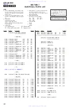

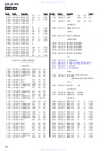


38
STR-KS1000
•
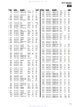
IC Pin Function Description
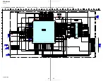
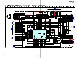
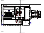
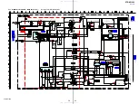
MAIN BOARD IC1501 CXD9862R (DIGITAL AUDIO SIGNAL PROCESSOR)
Pin No.
Pin Name
I/O
Description
1
VSS
-
Ground terminal
2
XRST
I
System reset signal input from the system controller "L": reset
3
EXTIN
I
Master clock signal input terminal Not used
4
LRCKI3
I
L/R sampling clock signal (44.1 kHz) input terminal Not used
5
VDDI
-
Power supply terminal (+1.8V)
6
BCKI3
I
Bit clock signal (2.8224 MHz) input terminal Not used
7
PLOCK
O
PLL lock signal output terminal Not used
8
VSS
-
Ground terminal
9
MCLK1
I
System clock input terminal (13.9 MHz)
10
VDDI
-
Power supply terminal (+1.8V)
11
VSS
-
Ground terminal
12
MCLK2
O
System clock output terminal (13.9 MHz)
13
MS
I
Master/slave setting terminal "L": internal clock, "H": external clock Fixed at "L" in this set
14
SCKOUT
O
Master clock signal output to the stream processor
15
LRCKI1
I
L/R sampling clock signal (44.1 kHz) input from the digital audio interface receiver
16
VDDE
-
Power supply terminal (+3.3V)
17
BCKI1
I
Bit clock signal (2.8224 MHz) input from the digital audio interface receiver
18
SDI1
I
Audio serial data input from the A/D converter
19
LRCKO
O
L/R sampling clock signal (44.1 kHz) output to the stream processor
20
BCKO
O
Bit clock signal (2.8224 MHz) output to the stream processor
21
VSS
-
Ground terminal
22
KFSIO
I
Audio clock signal input from the digital audio interface receiver
23 to 25
SDO1 to SDO3
O
Audio serial data output to the stream processor
26
SDO4
O
Audio serial data output terminal Not used
27
SPDIF
O
SPDIF signal output terminal Not used
28
LRCKI2
I
L/R sampling clock signal (44.1 kHz) input from the digital audio interface receiver
29
BCKI2
I
Bit clock signal (2.8224 MHz) input from the digital audio interface receiver
30
SDI2
I
Audio serial data input from the digital audio interface receiver
31
VSS
-
Ground terminal
32
HACN
O
Acknowledge signal output to the system controller
33
HDIN
I
Serial data input from the system controller
Serial data transfer clock signal input from the system controller
Serial data output to the system controller
Chip select input from the system controller
Write enable signal input from the system controller
SD-RAM chip enable output terminal Not used
Row address strobe signal output terminal Not used
42
GP15
Column address strobe signal output terminal Not used
43
OE0
O
Output of data input/output mask to the S-RAM
44
CS0
O
Chip select signal output to the S-RAM
45
WE0
O
Write enable signal output to the S-RAM
46
VDDE
-
Power supply terminal (+3.3V)
47
WMD1
I
External memory wait mode setting terminal Fixed at "H" in this set
48
VSS
-
Ground terminal
49
WMD0
I
External memory wait mode setting terminal Fixed at "H" in this set
50
PAGE2
O
External memory page selection signal output terminal Not used
www. xiaoyu163. com
QQ 376315150
9
9
2
8
9
4
2
9
8
TEL 13942296513
9
9
2
8
9
4
2
9
8
0
5
1
5
1
3
6
7
3
Q
Q
TEL 13942296513 QQ 376315150 892498299
TEL 13942296513 QQ 376315150 892498299


