— 54 —
I/O
I
I
I
I/O
I/O
I
I
I
O
I
I
I
O
—
—
I
I
I
I
I
I
O
O
O
O
O
O
I
I
Description
SDTO source select pin
“L”: internal ADC output, “H”: DAUX input
ORed with serial control register if P/S = “L” (Connected to ground)
MCKO clock frequency select pin
“L”: MCLK, “H”: MCLK/2. ORed with serial control register if P/S = “L” (Connected to ground)
Audio data master/slave mode select pin
“L”: slave mode, “H”: master mode (Connected to ground)
Audio serial data clock pin
Input/output channel clock pin
DAC1 audio serial data input pin
DAC2 audio serial data input pin
DAC3 audio serial data input pin
Audio serial data output pin
AUX audio serial data input pin (Connected to ground)
Double speed sampling mode pin
“L”: normal speed, “H”: double speed
ORed with serial control register if P/S = “L” (Connected to ground)
De-emphasis pin
ORed with serial control register if P/S = “L” (Connected to ground)
Master clock output pin (Not used)
Digital power supply pin
Digital ground pin
Power-down & reset pin
When “L”, the AK4526 is powered-down and the control registers are reset to default state.
If the state of P/S, M/S, CAD0-1 changes, then the AK4526 must be reset by PD.
X’tal oscillator select/test mode pin
“H”: X’tal oscillator selected
“L”: External clock source selected
“NC”: If pin is floating then test mode is enabled. (Connected to ground)
Input clock select 1 pin (Connected to ground)
Input clock select 0 pin (Connected to ground)
Chip address pin
Used during the serial control mode. (Connected to ground)
Chip address pin
Used during the serial control mode. (Connected to ground)
Lch #3 analog output pin
Rch #3 analog output pin
Lch #2 analog output pin
Rch #2 analog output pin
Lch #1 analog output pin
Rch #1 analog output pin
Lch analog negative input pin
Lch analog positive input pin
Pin Name
SDOS
MCLK
S/M
BCLK
LRCK
SDT11
SDT12
SDT13
SDTO
DAUX
DFS
DEM1 – DEM0
MCKO
D. 5V
D. GND
PD
TEST
ICKS1
ICKS0
CAD1
CAD0
LOUT3
ROUT3
LOUT2
ROUT2
LOUT1
ROUT1
LIN–
LIN+
Pin No.
1
2
3
4
5
6
7
8
9
10
11
12 – 13
14
15
16
17
18
19
20
21
22
23
24
25
26
27
28
29
30
IC1503
AK4526A A/D,D/A CONVERTER (DIGITAL BOARD)
Содержание STR-DB830 - Fm Stereo/fm-am Receiver
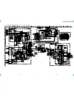
Страница 17: ...STR DB830 DB930 V929X 29 30 4 12 SCHEMATIC DIAGRAM SPEAKER SWITCH SECTION 26 26 ...
Страница 23: ...STR DB830 DB930 V929X 41 42 4 18 SCHEMATIC DIAGRAM VIDEO SECTION See page 59 for IC Block Diagrams ...
Страница 25: ...STR DB830 DB930 V929X 45 46 4 20 SCHEMATIC DIAGRAM MAIN SECTION 1 2 TO DIGITAL BOARD 3 3 PAGE 17 R401 1k ...


