


SPP-A973/A974
– 25 –
– 26 –
4-3. SCHEMATIC DIAGRAM — BASE MAIN SECTION (1/2) —
(Page 27)
Caution:
Pattern face side: Parts on the pattern face side seen from the
(Side B)
pattern face are indicated.
Parts face side: Parts on the parts face side seen from the
(Side A)
parts face are indicated.
THIS NOTE IS COMMON FOR PRINTED WIRING
BOARDS AND SCHEMATIC DIAGRAMS.
(In addition to this, the necessary note is
printed in each block.)
For schematic diagrams
• All capacitors are in µF unless otherwise noted. pF: µµF
50 WV or less are not indicated except for electrolytics
and tantalums.
• All resistors are in
Ω
and
1
/
4
W or less unless otherwise
specified.
•
C
: panel designation.
•
U
: B+ Line.
• Power voltage is dc 9 V and fed with regulated dc power
supply from external power voltage jack. (BASE PHONE)
• Power voltage is dc 12 V and fed with regulated dc power
supply from J1008 with 100
Ω
in series. (BASE PHONE)
• Power voltage is dc 3 V and fed with regulated dc power
supply from battery terminal. (HANDSET)
• Voltage is dc with respect to ground under no-signal
condition.
• Voltages are taken with a VOM (Input impedance 10 M
Ω
).
Voltage variations may be noted due to normal produc-
tion tolerances.
• Signal path.
N
: TX (To Tel Line)
O
: RX (From Tel Line)
P
: bell
For printed wiring boards
•
X
: parts extracted from the component side.
•
: Carbon pattern.
•
z
: Through hole.
•
b
: Pattern from the side which enables seeing.
(The other layer’s patterns are not indicated.)
Содержание SPP-A973 - Cordless Telephone With Answering System
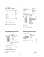
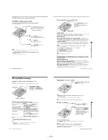
Страница 3: ... 3 SECTION 1 GENERAL This section is extracted from SPP A974 s instruction manual ...
Страница 4: ... 4 ...
Страница 5: ... 5 ...
Страница 6: ... 6 ...
Страница 7: ... 7 ...
Страница 8: ... 8 ...
Страница 9: ... 9 ...
Страница 10: ... 10 ...
Страница 11: ... 11 ...
Страница 12: ... 12 ...
Страница 13: ... 13 ...
Страница 14: ... 14 ...
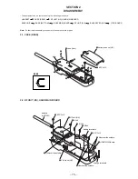
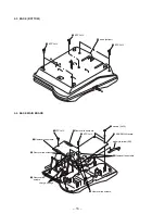
Страница 18: ... 18 2 7 I TAD BOARD 3 I TAD board BASE KEY board 2 BTP 3x12 1 Removal the solders ...
Страница 27: ...SPP A973 A974 4 7 SCHEMATIC DIAGRAM I TAD SECTION Refer to page 45 for IC Block Diagrams 35 36 Page 27 Page 39 ...
Страница 31: ...SPP A973 A974 4 11 SCHEMATIC DIAGRAM HAND MAIN SECTION Refer to page 45 for IC Block Diagrams 43 44 ...


