66
MZ-R910
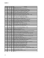
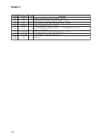
Pin No.
Pin Name
I/O
Description
242
A11
O
Address signal output terminal for D-RAM Not used
243
XOE
O
Output enable signal output terminal for D-RAM Not used
244
XWE
O
Data write enable signal output terminal for D-RAM Not used
245
TSTDR3
I
Test input terminal for D-RAM Not used
246
EVA
I
EVA/FLASH chip discrimination terminal “L”: FLASH chip, “H”: EVA chip
(fixed at “L” in this set)
247
FLASHVDD
—
Power supply terminal (for the built-in flash memory) (+2.2V)
248
FLASHVSS
—
Ground terminal (for the built-in flash memory)
249 to
256
NC
—
Not used
Содержание MZ-R910
Страница 75: ...75 MZ R910 MEMO ...


