56
MDX-M690
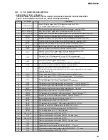
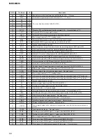
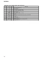
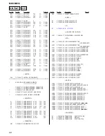
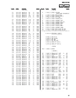
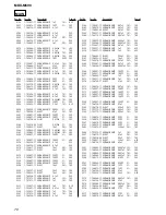
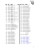
Pin No.
Pin Name
I/O
Description
53
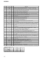
S-METER
I
FM and AM signal meter voltage detection signal input from the FM/AM tuner unit (TUX201)
(A/D input)
54
VCC
—
Power supply terminal (+5V)
55
ST-BY
O
Standby on/off control signal output to the power amplifier (IC309)
“L”: standby mode, “H”: amp on
56
NS-MASK
O
Discharge control signal output for the noise detection circuit “H”: discharge
57
DDC-ON
O
Power supply on/off control signal output of the power controller (IC101) “H”: power on
58
CD_EJECT_OK
O
Front panel open detection signal output to the MD mechanism controller (IC501)
“L”: eject possible
59
CD_OPEN_REQ
I
Mini-disc lock detection signal input to the MD mechanism controller (IC501)
60
NCO
O
Not used (open)
61
OPEN-KEY
I
Open key (LSW60) input terminal When “L” is input, open the front panel
62
NOSE-SW
I
Display panel attach detection signal input terminal “L”: front panel is attached
63
VSS
—
Ground terminal
64
DETACH_SW
I
Display panel detach detection signal input terminal “L”: front panel is detached
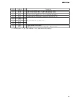
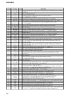
65
PWM
I
For frequency counting signal input teminal from the power controller (IC101)
66 to 68
NCO
O
Not used (open)
69
FLASH-W
I
Internal flash memory data write mode detection signal input terminal “L”: data write mode
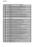
70
IIC-SDA
I/O
Two-way data IIC bus with the FM/AM tuner unit (TUX201), RDS decoder (IC202) and
TDA7406T (IC305)
71
IIC-SCL
O
IIC bus clock signal output to the FM/AM tuner unit (TUX201), RDS decoder (IC202) and
TDA7406T (IC305)
72
RC-IN1
I
Rotary remote commander shift key input terminal “L”: shift key on
73
X1A
O
Sub system clock output terminal (32.768 kHz)
74
X0A
I
Sub system clock input terminal (32.768 kHz)
75
DAVN
I
Synchronized detection signal of RDS data block input from the RDS decoder (IC202)
“H”: active
76
NCO
O
Not used (open)
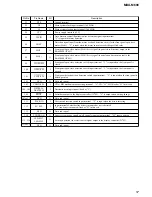
77
BUIN
I
Battery detection signal input from the SONY bus interface (IC601)
“L” is input at low voltage
78
NCO
O
Not used (open)
79
KEY_ACK
I
Input of acknowledge signal for the key entry Acknowledge signal is input to accept function
and eject keys in the power off status On at input of “H”
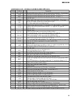
80
AD-ON
O
A/D converter power control signal output
When the KEY_ACK (pin
ul
) that controls reference voltage power for key A/D conversion
input is active, “L” is output from this terminal to enable the input
81
ACC IN
I
Accessory detect signal input terminal “L”: accessory on
82
FLS_PWON
O
Display power supply on/off control signal output “H”: display power on
83
P-ON
O
Audio power supply on/off control signal output “H”: audio power on
84
TEST-IN
I
Setting terminal for the test mode “L”: test mode, Normally: fixed at “H”
85
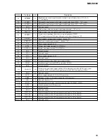
RAMBU
I
Internal RAM reset detection signal input from the reset signal generator (IC502)
Input terminal to check that RAM data are not destroyed due to low voltage
This checking is made within 100 msec after reset
86
HSTX
I
Hardware standby input terminal “L”: hardware standby mode Reset signal input in this set
87
MD2
I
Setting terminal for the CPU operational mode (fixed at “L” in this set)
88
MD1
I
Setting terminal for the CPU operational mode (fixed at “H” in this set)
89
MD0
I
Setting terminal for the CPU operational mode (fixed at “H” in this set)
90
RSTX
I
System reset signal input from the reset signal generator (IC502) and reset switch (SW901, S60)
“L”: reset “L” is input for several 100 msec after power on, then it changes to “H”
Содержание MDX-M690
Страница 79: ...79 MDX M690 MEMO ...

