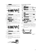
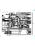

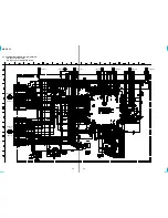

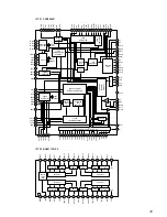

33
33
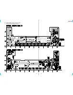
MDS-PC2
– MAIN SECTION –
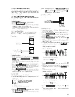
IC701
!£
(XOUT)
IC201
!™
(SYSCLK)
IC201
!¶
(LRCK1)
IC201
!§
(BCK)
– PANEL SECTION –
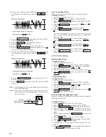
IC901
%•
(OSCO)
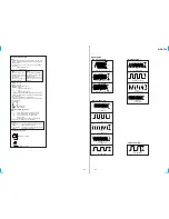
3.4Vp-p
2.822MHz
3.0Vp-p
22.581MHz
3.9Vp-p
2.4MHz
3.2Vp-p
10MHz
3.8Vp-p
44.1kHz
WAVEFORMS
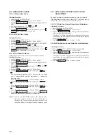
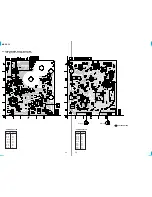
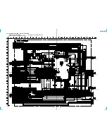
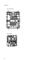
1
IC101
1
,
2
(I, J) (PLAY mode)
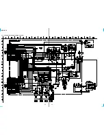
– BD (1/2) SECTION –
2
3
IC101
4
(A) (PLAY mode)
IC101
8
,
9
(E, F) (PLAY mode)
0.46Vp-p
0.1Vp-p
0.06Vp-p
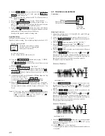
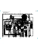
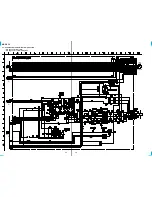
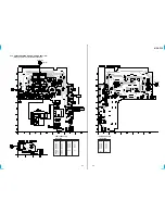
– BD (2/2) SECTION –
4
5
6
7
8
IC121
!§
(OSCI)
IC121
@¶
(LRCK)
IC121
@•
(XBCK)
IC121
@ª
(FS256)
IC121
(º
(FS4)
3.1Vp-p
22.581MHz
3.2Vp-p
44.1kHz
3.8Vp-p
2.822MHz
3.2Vp-p
176.4kHz
3.8Vp-p
11.29MHz
1
1
2
3
4
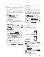
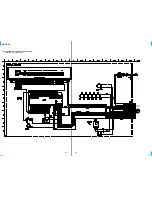
Note on Schematic Diagram:
Note:
• All capacitors are in µF unless otherwise noted. pF: µµF
50 WV or less are not indicated except for electrolytics
and tantalums.
• All resistors are in
Ω
and
1
/
4
W or less unless otherwise
specified.
•
¢
: internal component.
•
C
: panel designation.
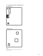
Note on Printed Wiring Boards:
Note:
•
X
: parts extracted from the component side.
•
Y
: parts extracted from the conductor side.
•
p
: parts mounted on the conductor side.
•
®
: Through hole.
•
b
: Pattern from the side which enables seeing.
(The other layers' patterns are not indicated.)
•
U
: B+ Line.
•
V
: B– Line.
•
H
: adjustment for repair.
no mark : STOP
(
) : Play the test disk (TDYS-1)
<
> : REC
∗
: Can not be measured.
• Voltages are taken with a VOM (Input impedance 10 M
Ω
).
Voltage variations may be noted due to normal produc-
tion tolerances.
• Waveforms are taken with a oscilloscope.
Voltage variations may be noted due to normal produc-
tion tolerances.
• Signal path.
E
: PB
: REC
p
: PB (digital out)
l
: REC (digital in)
Note:
The components identi-
fied by mark
!
or dotted
line with mark
!
are criti-
cal for safety.
Replace only with part
number specified.
Note:
Les composants identifiés par
une marque
!
sont critiques
pour la sécurité.
Ne les remplacer que par une
piéce por tant le numéro
spécifié.
Caution:
Pattern face side: Parts on the pattern face side seen from the
(Side B)
pattern face are indicated.
Parts face side:
Parts on the parts face side seen from the
(Side A)
parts face are indicated.
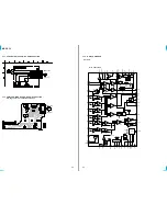
Q
C
E
B
C E
B
• Indication of transistor
These are omitted
These are omitted


