— 62 —
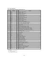
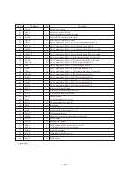
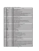
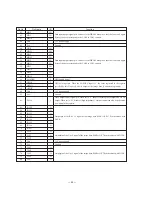
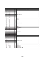
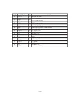
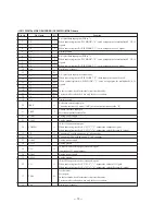
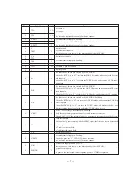
Pin Name
A18
A19
MPEG
MD0
MD1
φ
STBY
RESET
NM1
V
SS
EXTAL
XTAL
V
CC
AS
RD
WR
RESO
AV
SS
TEST0
TEST1
TEST2
SENS
DAC-SELECT
NPIN
CXD1853-SELECT
VREQ
VREF
AV
CC
CXD1913LTH
XHIRQ
SCOR
MREQ
DATA
AMUTE
LDON
XLT
SCLK
CLK
NP OUT
2545RST
Pin No.
41
42
43
44
45
46
47
48
49
50
51
52
53
54
55
56
57
58
59
60
61
62
63
64
65
66
67
68
69
70
71
72
73
74
75
76
77
78
79
80
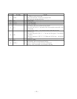
Function
Address bus output
MPEG wait input
Operation mode setting terminal (Connected to +5V)
Operation mode setting terminal (Connected to ground)
System clock output (Not used)
Shifts to the hardware standby mode when the standby terminal becomes “Low”.
(Unable to use H level fixed) (Connected to +5V)
Set into reset when the reset input pin becomes “Low”.
Requests mask disable interruption. (Unable to use H level fixed) (Connected to +5V)
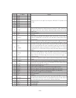
Ground
Connected to the Crystal oscillator. The EXTAL pin is also able to input external clocks.
Connected to the Crystal oscillator.
Connect to the power supply (+5V)
When the address strobe pin is “Low”, indicates that address outputs on the address bus are
valid.
When the read pin is “Low”, indicates that the external addresses space is in the read state.
When the read pin is “Low”, indicates that the external addresses space is in the write state
and the data bus are valid.
Reset output (Not used)
A/D converter (pin62-69) ground
Test 0 input
Test 1 input
Test 2 input
Internal state (SENSE) monitor input from BD boartd
Audio D/A converter select mode setting terminal
NTSC/PAL output mode setting terminal
CXD1853 select mode setting terminal (H:CXD1853 used)
Not used
A/D converter (pin62-69) reference voltage input (connected to +5V)
A/D converter (pin62-29) power supply (connected to +5V)
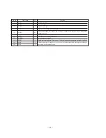
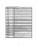
Serial data latch pulse output to CXD1913 (Digital NTSC/PAL encoder)
Interruption request input from MPEG decoder
Subcode sync input from BD board
Inputs command request from system controller
Serial data output to BD board, CXD1913 and CXD8567
Mute switching to BD board
Laser diode ON/OFF output
Latch output to BD board
SENS serial data reading clock output to BD board
Serial data clock output to BD board and CXD1913
NTSC/PAL output select
Digital signal processor (CXD2545Q system reset)
I/O
O
O
I
I
I
O
I
I
I
–
I
I
–
O
O
O
O
–
I
I
I
I
I
I
I
I
I
–
O
I
I
I
O
O
O
O
O
O
O
O
Содержание MCE-K700
Страница 8: ... 8 ...
Страница 9: ... 9 ...
Страница 10: ... 10 ...
Страница 11: ... 11 ...
Страница 12: ... 12 ...
Страница 13: ... 13 ...
Страница 14: ... 14 ...
Страница 15: ... 15 ...
Страница 16: ... 16 ...
Страница 21: ......
Страница 22: ......
Страница 23: ......
Страница 24: ......
Страница 25: ......
Страница 26: ......
Страница 27: ......

