


2
HCD-WZ5
Laser component in this product is capable
of emitting radiation exceeding the limit for
Class 1.
Notes on chip component replacement
Flexible Circuit Board Repairing
• Keep the temperature of soldering iron around 270˚C
during repairing.
• Do not touch the soldering iron on the same conductor of the
circuit board (within 3 times).
• Be careful not to apply force on the conductor when soldering
or unsoldering.
TABLE OF CONTENTS
1. GENERAL
·········································································· 4
2. DISASSEMBLY
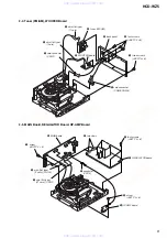
2-1. Case ··············································································· 7
2-2. Front Panel Assy ··························································· 8
2-3. PANEL Board, CD-TC-SW Board, ENTER-SW
Board, BACK-LIGHT Board, LCD Board ··················· 8
2-4. Tuner (FM/AM), WOOFER Board ······························ 9
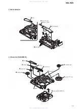
2-5. MAIN Board, REGULATOR Board, HP-AMP Board ··· 9
2-6. CD mechanism deck (CDM77B-K6BD47S) ·············· 10
2-7. Tray (AU) ···································································· 10
2-8. MS-128 Board ···························································· 11
2-9. Base Unit (BU-K6BD47S) ········································· 11
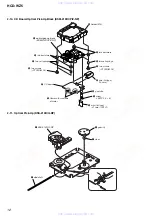
2-10. CD Board, Optical Pick-Up Block
(KSM-213DCP/Z-NP) ············· 12
2-11. Optical Pick-Up (KSS-213D/Q-RP) ··························· 12
3. ELECTRICAL ADJUSTMENTS
······························· 13
4. TEST MODE
···································································· 14
5. DIAGRAMS
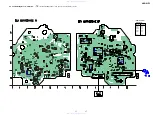
5-1. Circuit Boards Location ·············································· 15
5-2. Block Diagrams - Main Section - ······························· 16
5-3. Printed Wiring Board - CD Board - ···························· 17
5-4. Schematic Diagram - CD Board - ······························· 18
5-5. Printed Wiring Board - MAIN Section- ······················ 19
5-6. Schematic Diagram
- MAIN Section (1/2) - ··········· 20
- MAIN Section (2/2) - ··········· 21
5-7. Printed Wiring Board - PANEL Board - ····················· 22
5-8. Schematic Diagram - PANEL Board - ························ 23
5-9. Printed Wiring Board - LCD/SWITCH Section - ······· 24
5-10. Schematic Diagram - LCD/SWITCH Section - ·········· 25
5-11. Printed Wiring Board - REGULATOR Board - ·········· 26
5-12. Schematic Diagram - REGULATOR Board - ············ 27
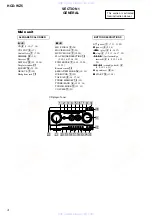
5-13. IC Block Diagrams ····················································· 28
5-14. IC Pin Function Description ······································· 29
6. EXPLODED VIEWS
6-1. Front Panel Section ····················································· 31
6-2. Chassis Section ···························································· 32
6-3. CD Mechanism Deck Section ····································· 33
6-4. KSM-213DCP/Z-NP ··················································· 34
7. ELECTRICAL PARTS LIST
······································· 35
The laser diode in the optical pick-up block may suffer electrostatic
break-down because of the potential difference generated by the
charged electrostatic load, etc. on clothing and the human body.
During repair, pay attention to electrostatic break-down and also
use the procedure in the printed matter which is included in the
repair parts.
The flexible board is easily damaged and should be handled with
care.
NOTES ON LASER DIODE EMISSION CHECK
The laser beam on this model is concentrated so as to be focused on
the disc reflective surface by the objective lens in the optical pick-
up block. Therefore, when checking the laser diode emission,
observe from more than 30 cm away from the objective lens.
NOTES ON HANDLING THE OPTICAL PICK-UP
BLOCK OR BASE UNIT
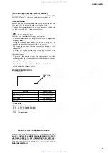
This appliance is
classified as a CLASS 1
LASER product. This
label is located on the
rear exterior.
The following caution label is located inside the apparatus.
www. xiaoyu163. com
QQ 376315150
9
9
2
8
9
4
2
9
8
TEL 13942296513
9
9
2
8
9
4
2
9
8
0
5
1
5
1
3
6
7
3
Q
Q
TEL 13942296513 QQ 376315150 892498299
TEL 13942296513 QQ 376315150 892498299


