17
HCD-PX333
SECTION 2
GENERAL
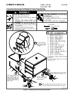
4
Main unit
1
qj
qk
qh qg qf qd qs qa
q;
ws
wa
w;
ql
2
3
4
5
6
7
8
9
CD disc tray
9
(8)
CD SYNC HIGH
q;
(17)
CD SYNC NORMAL
qa
(17)
CD
N X
ws
(9)
Display window
3
FUNCTION
qh
(9, 13, 18, 25, 41)
MD insertion slot
2
(13)
MD
NX
6
(13)
PHONES jack
qj
PLAY MODE
qg
(9, 13, 24)
REC/REC IT
qs
(18)
REC MODE
qd
(20)
REPEAT
qf
(9, 14)
STEREO/MONO
ql
(35)
TUNER/BAND
qd
(34)
TUNING MODE
qg
(34)
/–
w;
(34)
/–
qk
BUTTON DESCRIPTIONS
1
Z
MD
4
x
(MD)
5
m/M
(MD)
7
./>
(MD)
7
Z
CD
8
m/M
(CD)
w;
./>
(CD)
w;
x
(CD)
ws
?/1
The items are arranged in alphabetical order. Refer to the pages indicated in parentheses for details
Parts Identification
This section is extracted
from instruction manual.
Содержание HCD-PX333
Страница 49: ...49 HCD PX333 Checking Location IC171 IC101 TP VC TP FE TP TE TP RF BD CD BOARD Conductor Side ...
Страница 50: ...50 HCD PX333 MEMO ...
Страница 63: ...63 63 HCD PX333 6 10 SCHEMATIC DIAGRAM MD DIGITAL SECTION 2 3 IC B D See page 79 for IC Block Diagrams ...
Страница 64: ...64 64 HCD PX333 6 11 SCHEMATIC DIAGRAM MD DIGITAL SECTION 3 3 IC B D IC B D See page 79 for IC Block Diagrams ...
Страница 66: ...66 66 HCD PX333 6 13 SCHEMATIC DIAGRAM MAIN BOARD 1 2 See page 80 for IC Block Diagrams IC B D IC B D ...
Страница 69: ...69 69 HCD PX333 6 17 SCHEMATIC DIAGRAM AMP BOARD ...
Страница 70: ...70 70 HCD PX333 6 18 SCHEMATIC DIAGRAM SP BOARD ...
Страница 72: ...72 72 HCD PX333 6 20 SCHEMATIC DIAGRAM PANEL SECTION1 ...
Страница 75: ...75 75 HCD PX333 6 24 SCHEMATIC DIAGRAM POWER BOARD ...
Страница 111: ...111 HCD PX333 MEMO ...