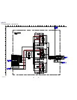

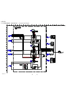


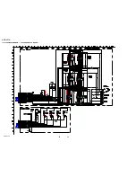


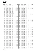

58
HCD-LF1H
Pin No.
Pin Name
I/O
Description
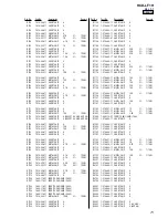
114
XIFSSY
I
DQM signal input
115
RD7
I/O
Data bus 7 from SD-RAM (IC104)
116
DVSS
—
Ground terminal
117, 118
RD 6, 5
I/O
Data bus 6, 5 from SD-RAM (IC104)
119
DVSS
—
Ground terminal
120, 121
RD 4, 3
I/O
Data bus 4, 3 from SD-RAM (IC104)
122
DVDD18
—
Power supply (+1.8V from IC110)
123 to 125
RD 2 to 0
I/O
Data bus 2 to 0 from SD-RAM (IC104)
126
RD15
I/O
Data bus 15 from SD-RAM (IC104)
127
DVDD3
—
Power supply (SW+3.3V)
128
RD 14
I/O
Data bus 14 from SD-RAM (IC104)
129 to 133
RD 13 to 9
I/O
Data bus 13 to 9 from SD-RAM (IC104)
134
DVSS
—
Ground terminal
135
RD8
I/O
Data bus 8 from SD-RAM (IC104)
136
WAIT SW
I
WAITSW signal input
137
DQM1
O
DQM1 signal output to SD-RAM (IC104)
138
RWE
O
WE signal output to SD-RAM (IC104)
139
CAS
O
CAS signal output to SD-RAM (IC104)
140
RAS
O
RAS signal output to SD-RAM (IC104)
141
DVDD3
—
Power supply (SW+3.3V)
142
RCS
O
RCS signal output to SD-RAM (IC104)
143
BA0
O
BAO signal output to SD-RAM (IC104)
144
DVSS
—
Ground terminal
145
BA1
O
BA1 signal output to SD-RAM (IC104)
146
RA10
O
Address bus 10 output to SD-RAM (IC104)
147
RA0
O
Address bus 0 output to SD-RAM (IC104)
148
DVSS
—
Ground terminal
149 to 151
RA 1 to 3
O
Address bus 1 to 3 output to SD-RAM (IC104)
152
DVDD18
—
Power supply (+1.8V from IC110)
153
RVREF
—
Reference voltage (not used)
154
RCLKB
—
Dram clock (not used)
155
DVDD3
—
Power supply (SW+3.3V)
156
DRCLK
O
CLK signal output to SD-RAM (IC104)
157
CKE
O
CKE signal output to SD-RAM (IC104)
158 to 160
RA 11, 9, 8
O
Address bus 11, 9, 8 output to SD-RAM (IC104)
161
DVSS
—
Ground terminal
162
RA7
O
Address bus 7 output to SD-RAM (IC1104)
163
DVSS
—
Ground terminal
164 to 166
RA 6 to 4
O
Address bus 6 to 4 output to SD-RAM (IC104)
167
DVDD3
—
Power supply (SW+3.3V)
168 to 172
SMPTE_Y (7) to Y (3)
O
VIDEO signal output to HDMI Driver (IC701)
173
DVDD18
—
Power supply (+1.8V from IC110)
174
SMPTE_Y (2)
O
VIDEO signal output to HDMI Driver (IC701)
175
DVSS
—
Ground terminal
176 to 177
SMPTE_Y (1) to Y (0)
O
VIDEO signal output to HDMI Driver (IC701)
178
VCLK
O
System clock output
179
WIDE
O
Wide switch signal output
180
CK RW SW
I
CK RW SW signal input
181
NC
O
TSDM signal output to Motor Driver (IC201) (not used)
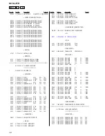
Содержание HCD-LF1H
Страница 78: ...78 HCD LF1H MEMO ...