


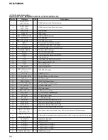


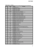

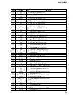


88
HCD-FX900W
Pin No.
Pin Name
I/O
Description
48
MSW
O
Mute signal control output
49
CKSW
—
Not used
50
OCSW
I
Servo 1
51
EEWP
O
WF signal output to EEPROM (IC103)
52
DVDD18
—
Power supply (+1.8V from IC110)
53 to 59
HA 2 to 8
O
Address bus 2 to 8 output to FLASH ROM (IC102)
60, 61
HA18, 19
O
Address bus 18, 19 output to FLASH ROM (IC102)
62
DVSS
—
Ground terminal
63
APLLCAP
I
APLL external capacitance connection
64
APLLVSS
—
Ground terminal
65
VDD3
—
Power supply (+3.3V from IC105)
66
XWR
O
WE signal output to FLASH ROM (IC102)
67 to 72
HA 16 to 11
O
Address bus 16 to 11 output to FLASH ROM (IC102)
73
DVDD3
—
Power supply (SW+3.3V)
74, 75
HIGHA 10, 9
O
Address bus 10, 9 output to FLASH ROM (IC102)
76
HA20
O
Address bus 20 output to FLASH ROM (IC102)
77
XROMCS
O
CE signal output to FLASH ROM (IC102)
78
HA1
O
Address bus 1 output to FLASH ROM (IC102)
79
XRD
O
OE signal output to FLASH ROM (IC102)
80
DVDD3
—
Power supply (SW+3.3V)
81 to 84
HD 0 to 3
I
Data bus 0 to 3 input from FLASH ROM (IC102)
85
DVSS
—
Ground terminal
86 to 88
HD 4 to 6
I
Data bus 4 to 6 input from FLASH ROM (IC102)
89
HA21
O
Address bus 21 output to FLASH ROM (IC102)
90
ALE
O
Address latch enable (not used)
91
HD7
I
Data bus 7 input from FLASH ROM (IC102)
92
HA17
O
Address bus 17 output to FLASH ROM (IC102)
93
HA0
O
Address bus 0 output to FLASH ROM (IC102)
94
DVSS
—
Ground terminal
95
UWR
I
System controller write strobe (not used)
96
URD
I
System controller read strobe (not used)
97
DVDD18
—
Power supply (+1.8V from IC110)
98
IFSDO
O
DVD SOD signal output to system controller (IC501)
99
IFSCK
O
DVD SCO signal output to system controller (IC501)
100
XIFCS
I
DVD XIFCS signal input from system controller (IC501)
101
IFSDI
I
VIFBUSY signal input from system controller (IC501)
102
SCL
O
SCL signal output to EEPROM (IC103)
103
SDA
O
SDA signal output to EEPROM (IC103)
104
TRG-SW
O
RS232 RXD signal output (not used)
105
XRST
O
RS232 reset signal output
106
RXD
I
RD232 RXD clock
107
TXD
O
RD232 TXD data
108
DVDD3
—
Power supply (SW+3.3V)
109
ICE
I
ICE mode enable (not used)
110
XSYSRST
I
MTRST signal input from system controller (IC501)
111
IR
I
IR control signal input (not used)
112
XTXINT
I
External interrupt0 (not used)
113
DQMO
O
DQM0 signal output to SD-RAM (IC104)
114
XIFSSY
I
DQM signal input


