- 25 -
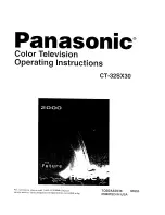
5-1. BLOCK DIAGRAMS (2)
A 2/2 ( )
9
7
8
RELAY
SWITCH
Q6001
T6003
SRT
16
15
17
18
18
16
2
15
2
IC6002
ERROR AMP
PH6101
PHOTO COUPLER
AUDIO VCC
LOWB
+3.3V
7
5
IC5001
V OUTPUT
3
1
VD+
BOOST
REF
OUT
PIN OUT
Q5032
6
4
3
2
1
5
T5011
FBT
FV
ABL
12
3
4
5
6
13
8
9
11
10
7
V- DY+
V- DY-
H- DY+
H- DY+
TO C BOARD
CN7007
H1
200V
TO PICTURE
TUBE
2
3
6
5
+
-
+
-
1
7
IC5031
PIN CORRECTION
EW
HP
PROTECT
IN
VP
VD-
4
1
2
3
T5031
HDT
HD
T6102
CN6001
VD
VG(H)
VS
+B
HV
CN5008
IC6001
D5014
-15V RECT
1
2
1
3
DGC
DGC
DGC
DGC CHECK
DGC CHECK
CN6003
CN6002
2
1
H- DY-
H- DY-
TO C BOARD
CN7006
G2
D6025
D6008
LINE
FILTER
T6001
RELAY
RY6001
1
3
4
6
7
9
CT
VSENSE
RT
TIMER
SS
OCP
12
VG(L)
MAIN RECT
D6001
Q6006
7
3
LOWB
D6018
D6019
QCP DETECT
Q6002, 6003
H-DRIVE
Q5035
2
FB
D5013
+15V RECT
5
1
2
VARISTOR
8
Q6007
H-OUT
Q5033
CN5001
O
I
D6038
TO A 1/2
POWER SUPPLY,
DEFLECTION, VIDEO, AUDIO
POWER
S6001
RECT
1
1
12
10
11
8
6
5
4
1
4
1
5V REG
3.3V REG
IC6005
IC6008
STBY
+5V
D6125
D6126
F6001
TO C BOARD
FOCUS
STBY
VDY
HDY
DY ASSY
VC1