


4-31
DSC-N1_L2
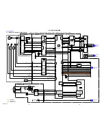
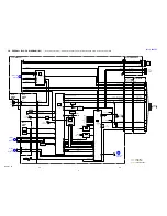
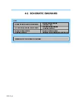
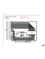
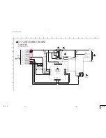
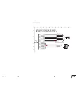
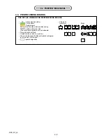
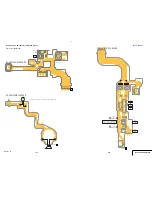
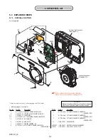
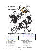
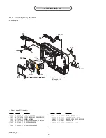
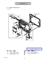
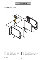
4-3. PRINTED WIRING BOARDS
4-3. PRINTED WIRING BOARDS
•
: Uses unleaded solder.
•
: Circuit board
: Flexible board
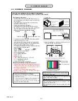
Pattern from the side which enables seeing.
: pattern of the rear side
(The other layers’ patterns are not indicated)
• Through hole is omitted.
• Circled numbers refer to waveforms.
• There are a few cases that the part printed on diagram
isn’t mounted in this model.
•
C
: panel designation
THIS NOTE IS COMMON FOR PRINTED WIRING BOARDS
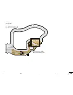
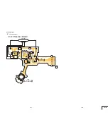
2
1
3
2
1
3
2
1
3
3
4
5
2
1
1
2
3
6
5
4
E
B
C
3
1
5
2
4
6
1
2
3
6
5
4
3
1
5
2
4
6
1
2
3
5
4
4
3
1
2
3
1 2
4
5
5
3 4
1
2
1
4
2
3
4
6
2
5
3
1
1
2
4
3
1
4
2
3
• Chip parts.
Transistor
Diode
4-3. PRINTED WIRING BOARDS
Содержание DSC-N1
Страница 25: ...HELP DSC N1_L2 CCD block 2 1 CCD block Sheet CD CD 585 ...
Страница 26: ...DSC N1_L2 Link Link 3 BLOCK DIAGRAMS OVERALL BLOCK DIAGRAM 2 2 OVERALL BLOCK DIAGRAM 1 2 POWER BLOCK DIAGRAM ...
Страница 45: ...4 45 DSC N1_L2 Waveforms of the SY 138 board are not shown Page 4 43 is not shown ...


