


3
CAUTION
Use of controls or adjustments or performance of procedures
other than those specified herein may result in hazardous
radiation exposure.
CX-VX55/VX77
NOTES ON HANDLING THE OPTICAL PICK-UP BLOCK
OR BASE UNIT
The laser diode in the optical pick-up block may suffer electrostatic
breakdown because of the potential difference generated by the
charged electrostatic load, etc. on clothing and the human body.
During repair, pay attention to electrostatic break-down and also
use the procedure in the printed matter which is included in the
repair parts.
The flexible board is easily damaged and should be handled with
care.
NOTES ON LASER DIODE EMISSION CHECK
The laser beam on this model is concentrated so as to be focused on
the disc reflective surface by the objective lens in the optical pick-
up block. Therefore, when checking the laser diode emission,
observe from more than 30 cm away from the objective lens.
Laser component in this product is capable
of emitting radiation exceeding the limit for
Class 1.
This appliance is
classified as a CLASS 1
LASER product. The
label is located on the
left side of the unit as
viewed from the front.
TABLE OF CONTENTS
1. GENERAL
Front Panel Controls ................................................................ 4
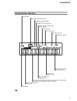
Display Window Indicators ..................................................... 5
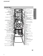
Remote Control ....................................................................... 6
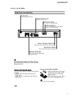
Rear Panel Connections (AEP, UK, CET, RU Model) ............ 7
Rear Panel Connections (E3, E41, AUS, SP Model) ............... 8
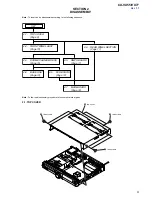
2. DISASSEMBLY
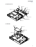
2-1. Top Cover ............................................................................ 9
2-2. Front Panel Assy ............................................................... 10
2-3. DVD Mechanism Deck ..................................................... 10
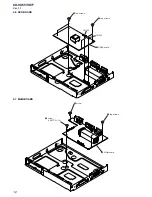
2-4. Rear Panel Section ............................................................ 11
2-5. SMPS Board ...................................................................... 11
2-6. DVD Board ....................................................................... 12
2-7. Main Board ....................................................................... 12
2-8. Base Unit ........................................................................... 13
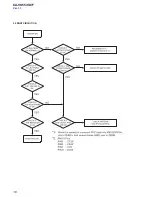
3. ELECTRICAL TROUBLESHOOTING GUIDE
3-1. Audio Part .......................................................................... 14
3-2. DVD Part ........................................................................... 18
3-3. Details and Waveforms on System Test and Debugging ... 25
4. TEST MODE
..................................................................... 38
5. ELECTRICAL ADJUSTMENT
.................................... 39
6. DIAGRAMS
6-1. Block Diagram –DVD Section– ........................................ 41
6-2. Block Diagram –Audio Section– ...................................... 42
6-3. Block Diagram –Tuner/Power Section– ............................ 43
6-4. Printed Wiring Boards –DVD Section (1/2)– .................... 45
6-5. Printed Wiring Board –DVD Section (2/2)– ..................... 46
6-6. Schematic Diagram –DVD Section (1/3)– ........................ 47
6-7. Schematic Diagram –DVD Section (2/3)– ........................ 48
6-8. Schematic Diagram –DVD Section (3/3)– ........................ 49
6-9. Printed Wiring Board –Main Section (1/2)– ..................... 50
6-10. Printed Wiring Board –Main Section (2/2)– ..................... 51
6-11. Schematic Diagram –Main Section (1/5)– ........................ 52
6-12. Schematic Diagram –Main Section (2/5)– ........................ 53
6-13. Schematic Diagram –Main Section (3/5)– ........................ 54
6-14. Schematic Diagram –Main Section (4/5)– ........................ 55
6-15. Schematic Diagram –Main Section (5/5)– ........................ 56
6-16. Printed Wiring Board –Display Section– .......................... 57
6-17. Schematic Diagram –Display Section– ............................. 58
6-18. Printed Wiring Board –Key Section– ................................ 59
6-19. Schematic Diagram –Key Section– ................................... 60
6-20. Printed Wiring Board –Power Section– ............................ 61
6-21. Schematic Diagram –Power Section– ............................... 62
7. EXPLODED VIEWS
7-1. Front Panel Section ........................................................... 67
7-2. Boards Section .................................................................. 68
7-3. DVD Mechanism Section .................................................. 69
8. ELECTRICAL PARTS LIST
........................................ 70
Ver. 1.1
Содержание CX-VX55
Страница 16: ...16 CX VX55 VX77 Ver 1 1 3 FRONT CIRCUIT 1 2 ...
Страница 17: ...17 CX VX55 VX77 Ver 1 1 4 FRONT CIRCUIT 2 2 ...
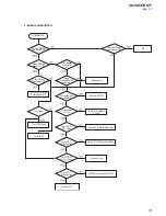
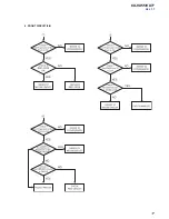
Страница 19: ...19 CX VX55 VX77 Ver 1 1 2 Test debug flow ...
Страница 20: ...20 CX VX55 VX77 Ver 1 1 ...
Страница 21: ...21 CX VX55 VX77 Ver 1 1 ...
Страница 22: ...22 CX VX55 VX77 Ver 1 1 ...
Страница 23: ...23 CX VX55 VX77 Ver 1 1 ...
Страница 24: ...24 CX VX55 VX77 Ver 1 1 ...
Страница 28: ...28 CX VX55 VX77 Ver 1 1 2 Tray close waveform 3 Tray open waveform ...
Страница 30: ...30 CX VX55 VX77 Ver 1 1 6 LASER POWER CONTROL RELATED SIGNAL NO DISC CONDITION 7 DISC TYPE JUDGEMENT WAVEFORM ...
Страница 31: ...31 CX VX55 VX77 Ver 1 1 ...
Страница 32: ...32 CX VX55 VX77 Ver 1 1 8 FOCUS ON WAVEFORM ...
Страница 33: ...33 CX VX55 VX77 Ver 1 1 9 SPINDLE CONTROL WAVEFORM NO DISC CONDITION ...
Страница 34: ...34 CX VX55 VX77 Ver 1 1 10 TRACKING CONTROL RELATED SIGNAL SYSTEM CHECKING ...
Страница 35: ...35 CX VX55 VX77 Ver 1 1 11 RF WAVEFORM 12 MT1379 AUDIO OPTICAL AND COAXIAL OUTPUT ASPDIF ...
Страница 36: ...36 CX VX55 VX77 Ver 1 1 13 MT1379 VIDEO OUTPUT WAVEFORM 1 Full colorbar signal CVBS 2 Y ...
Страница 37: ...37 CX VX55 VX77 Ver 1 1 3 C 14 AUDIO OUTPUT FORM AUDIO DAC 1 Audio related Signal ...
Страница 40: ...40 CX VX55 VX77 Ver 1 1 MEMO ...


