33
33
CDX-M610
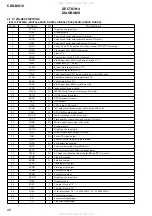
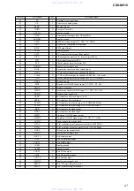
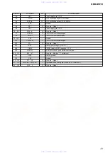
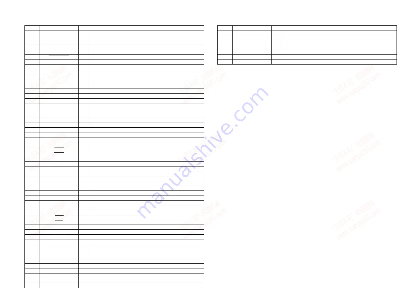
Pin No.
Pin Name
I/O
Pin Description
112
4V SEL
I
4 V select input (Not used in this set.)
113
(P-SEL)
I
Power select initial setting (Fixed at “L” in this set.)
114
TUNON
O
Tuner power control output
115, 116
LED SW1, 2
O
Operation/display side illumination select control output 1, 2
117, 118
(NCO)
O
Not used. (Open)
119
VSS
—
Ground
120
(DOLBY)
O
DOLBY B ON/OFF select output (“H”: ON) (Not used in this set.)
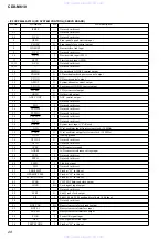
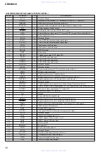
Pin No.
Pin Name
I/O
Pin Description
54
VCC
—
Power supply pin (+5 V)
55
ST-BY
O
Power amplifier drive output
56
NS MASK
O
Noise detection output (Not used in this set.)
57
(REEL)
I
Tape rotation detection input (Fixed at “L” in this set.)
58
CD EJECTOK
O
CD eject control output (Not used in this set.)
59
CD OPENREQ
I
Front panel open request input
60 – 62
(POS0 – 2)
I
Mechanism deck position detection input (Fixed at “L” in this set.)
63
VSS
—
Ground
64
(POS3)
I
Mechanism deck position detection input (Fixed at “L” in this set.)
65
PWM
I
Oscillation frequency count input
66
(LMLOD)
O
Loading motor control output (Loading direction) (Not used in this set.)
67
(CM-ON)
O
Capstan motor drive power supply output (Not used in this set.)
68
(TAPEON)
O
Tape drive power supply output (Not used in this set.)
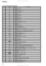
69
FLASH-W
I
Flash write input
70
I2CSIO
I/O
I
2
C BUS serial data input/output
71
I2CCKO
O
I
2
C BUS serial clock output
72
RC IN1
I
Rotary commander input 1
73
X1A
O
Sub ceramic oscillator output (32 kHz)
74
X0A
I
Sub ceramic oscillator input (32 kHz)
75
DAVN
I
RDS IC data acquisition detection input (Not used in this set.)
76
CDON-IN
I
CD mechanism power control input (Not used in this set.)
77
BU IN
I
Backup power detection input
78
DSPREADY
I
Digital signal processor ready input (Not used in this set.)
79
KEY ACK
I
Key input acknowledge
80
ADON
O
Power control output of A/D converter.
81
ACCIN
I
Accessory key ON input
82
FLSW PWON
O
Flash power ON output
83
PW ON
O
System power control output
84
TESTIN
I
Test mode initial setting detection input
85
RAM BU
I
RAM reset detection input
86
HSTX
I
Hardware standby input (Connect to pin
o;
(RSTX).)
87
MD2
I
Operation mode input (Connect to ground in this set.)
88, 89
MD1, 0
I
Operation mode input (Connect to VCC in this set.)
90
RSTX
I
Reset input
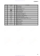
—
Ground
I
Main ceramic oscillator input (3.68 MHz)
O
Main ceramic oscillator output (3.68 MHz)
—
Power supply pin (+5 V)
I
Illumination control input
I
Front panel OPEN/CLOSE motor current abnormal detection input
O
Front panel OPEN/CLOSE motor control output (– direction)
O
Front panel OPEN/CLOSE motor control output (+ direction)
I
Front panel CLOSE detection switch input
I
Front panel OPEN detection switch input
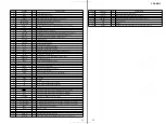
101 – 103
SCODE0 – 2
I
Security code setting port 0 – 2 (Fixed at “L”)
104
DSTSETTING1
I
Destination setting port (Fixed at “L” in TYPE A, fixed at “H” in TYPE B.)
105
DSTSETTING2
I
Destination setting port (Fixed at “L” in TYPE A, fixed at “H” in TYPE B.)
106
BOOT
O
Display micon write control output
107
(NCO)
I
Not used. (Open)
108
DSPON
O
Digital signal processor power control output (Not used in this set.)
109
(NCO)
O
Not used. (Open)
110
EMPH-IN
I
Emphasis input (Not used in this set.)
111
(PACKSW)
I
Tape with/without detection input (Not used. (Fixed at “L” in this set.))
w w w . x i a o y u 1 6 3 . c o m
Q Q 3 7 6 3 1 5 1 5 0
9
9
2
8
9
4
2
9
8
T E L
1 3 9 4 2 2 9 6 5 1 3
9
9
2
8
9
4
2
9
8
0
5
1
5
1
3
6
7
3
Q
Q
TEL 13942296513 QQ 376315150 892498299
TEL 13942296513 QQ 376315150 892498299

