— 17 —
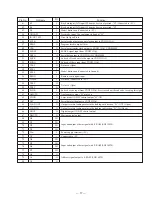
Pin Name
K3
K4
K5
ADJ/AFJ
IN/OUT SW
SCLK
PRGL
CLK
SENSE
DATA
SQCK
SUBQ
TEST
SEL 1
SEL 0
RMIN
TIMER
TEST
TEST
SCOR
AMUTE
LDON
XLT
LOAD OUT
LOAD IN
DOUT
DMUTE
D0
D1
D2
D3
V
DD
NC
D4
D5
D6
D7
A0
A1
A2
Pin No.
41
42
43
44
45
46
47
48
49
50
51
52
53
54
55
56
57
58
59
60
61
62
63
64
65
66
67
68
69
70
71
72
73
74
75
76
77
78
79
80
I/O
I
I
I
I
I
O
O
O
I
O
O
I
O
I
I
I
I
O
O
I
O
O
O
O
O
O
O
I/O
I/O
I/O
I/O
I
–
I/O
I/O
I/O
I/O
O
O
O
Function
Key data input (A/D input). When the key is not pressed: “H” (Connected to +5V)
Key data input (A/D input). When the key is not pressed: “H”
Model distinction (Connected to +5V)
Test mode input. The equipment is fixed at “H”
Disc lid Open/Close
Serial read out data read out clock output to CXD2515AQ
Program latch to digital filter
Serial data transfer clock output to CXD2515AQ, CXD8504M
SENSE signal input from CXD2515AQ
Serial data output to CXD2515AQ, CXD8504M
Sub code Q read out clock output to CXD2515AQ
Sub code Q data input from CXD2515AQ
Not used (Open)
Model distinction (Connected to Ground)
Remote contrl signal input
Not used (Connected to +5V)
Not used (Open)
Sub code sync input from CXD2515AQ. Start to read out the sub code receiving this signal
Analog mute output. “H” mute on
Laser diode ON/OFF control output “H”: ON
Serial data latch output to CXD2515AQ
Output to rotate loading motor in the loading out direction. “H”: OUT (Open)
Output to rotate loading motor in the loading in direction. “H”: IN (Open)
Digital output ON/OFF control output
Muting control output
Input and output of data signal with S. RAM (LH5160T4)
Power supply terminal (+5V)
Connected to +5V
Input and output of data signal with S. RAM (LH5160T4)
Address signal output to S. RAM (LH5160T4)


