background image

– 54 –

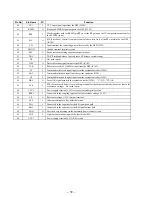
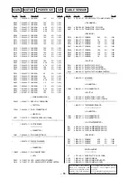
Pin No.

Pin Name

I/O

Function

49

SQOUT

I

Subcode Q data input from the DSP (IC102)

50

COIN

O

Command serial data output to the RF amplifier (IC101) and DSP (IC102)

51

SCLK

O

Serial data transfer clock signal output to the CD text decoder (IC104)    “L” active

52

SRDT

I

Serial data input from the CD text decoder (IC104)

53

NC

O

Not used (open)

54

DRF

I

Focus OK signal input from the RF amplifier (IC101) and DSP (IC102)    “L”: NG, “H”: OK

55

WRQ

I

Subcode Q synchronizing signal input from the DSP (IC102)    “H” active

56

RMIN

I

Remote control signal input from the remote control receiver (IC902)    “L” active

57

TGL

I

Tracking gain control signal input from the DSP (IC102)                                                                   
Gain becomes low when tracking gain is “H”

58

RWC

O

Command latch output to the RF amplifier (IC101) and DSP (IC102)    “L” active

59

SL–

O

Sled feeding signal (internal direction) output to the RF amplifier (IC101)    “H” active

60

DQSY

I

Serial data synchronizing signal input from the CD text decoder (IC104)    “L” active

61

XMODE

O

Reset signal output to the CD text decoder (IC104)    “H”: reset

62

T.SENS1

I

Disc table flag detect sensor (IC51) input terminal

63

T.SENS2

I

Disc table flag detect sensor (IC52) input terminal

64

T.SENS3

I

Disc table home position detect sensor (IC53) input terminal

65

DOWNSW

I

Inputs the loading out switch (S52) detection signal    “L” active

66

UPSW

I

Inputs the loading in switch (S51) detection signal    “L” active

67

SELECT

I

Not used (fixed at “H”)

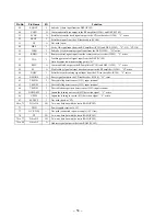
68 to 71

D3 to D6

I/O

Two-way data bus with the static RAM (IC502)

72

VDD

Power supply terminal (+5V)

73

NC (VDD)

Not used (connected to power supply (+5V) line)

74

D7

I/O

Two-way data bus with the static RAM (IC502)

75 to 77

D0 to D2

I/O

Two-way data bus with the static RAM (IC502)

78 to 80

A0 to A2

O

Address signal output to the static RAM (IC502)

Содержание CDP-CX57 - 50 Disc Cd Changer

Страница 1: ...S 213B S N Jack Maximum Load impedance type output level LINE OUT Phono 2V Over 10 kilohms Jacks at 50 kilohms DIGITAL Optical 18 dBm Wave length 660 nm OUT output OPTICAL connector Where purchased Power requirements US Canada 120 V AC 60 Hz Australia 240 V AC 50 60 Hz UK 220 V 230 V AC 50 60 Hz Other countries 110 V 120 V or 220 V 240 V AC adjustable 50 60 Hz General Power requirements Power cons...

Страница 2: ...uct The CLASS 1 LASER PRODUCT MARKING is located on the rear exterior 4 997 568 0π 4 997 568 1π 4 997 568 2π 4 997 568 3π 4 997 568 4π 4 997 568 5π 4 997 568 6π US model Canadian model AEP AED model UK model Australian model E model Singapore model PART No MODEL MODEL IDENTIFICATION BACK PANEL Abbreviation AED North European PART No CAUTION INVISIBLE LASER RADIATION WHEN OPEN AND INTERLOCKS DEFEAT...

Страница 3: ...A battery operated AC milliammeter The Data Precision 245 digital multimeter is suitable for this job 3 Measuring the voltage drop across a resistor by means of a VOM or battery operated AC voltmeter The limit indica tion is 0 75 V so analog meters must have an accurate low voltage scale The Simpson 250 and Sanwa SH 63Trd are ex amples of a passive VOM that is suitable Nearly all battery operated ...

Страница 4: ...ce or a character resembling it For details refer to Table 2 CD TEXT DISC Recorded Contents and Display Table 1 CD TEXT TEST DISC TEXT Data Contents TRACKS No 1 to 41 Normal Characters 1 1kHz 0dB L R 22 1kHz 90dB L R 2 20Hz 0dB L R 23 Infinity Zero w o emphasis L R 3 40Hz 0dB L R 24 Infinity Zero with emphasis L R 4 100Hz 0dB L R 25 400Hz 7kHz 4 1 0dB L R 5 200Hz 0dB L R 26 400Hz 7kHz 4 1 10dB L R...

Страница 5: ... C ª P R are not displayed 56 2 3 µ B0h to B7h µ B0 2 3 are not displayed 57 1 º B8h to BFh B8 1 º are not displayed 58 À Á Â Ã Ä ÅÆÇ C0h to C7Fh ÀÁ Â Ã Ä ÅÆÇ C0h to C7h 59 È É Ê Ë Ì Í Î Ï C8h to CFh N All the same 60 D Ñ Ò Ó Ô Õ Ö D0h to D7Fh D ÑÒÓ Ô Õ Ö D0h to D7h 61 Ø Ù Ú Û Ü Y ß D8h to DFh Ù Ú Û Ü Y ß D8 62 à á â ã ä å æ ç E0h to E7h à á â ã ä å æ ç E0h to E7h 63 è é ê ë ì í î ï E8h to EFh N A...

Страница 6: ...CHARACTER PUSH ENTER knob FADER button LOCATION OF PARTS AND CONTROLS Front Panel CHECK button CLEAR button button button p button P button ª button º PLUS ONE button X FADE button NO DELAY button MEGA CONTROL button PUSH OPEN STANDBY 1 u PULS ONE PLAY MODE REPEAT GROUP FILE 1 2 3 GROUP 4 5 CHECK FADER CLEAR PUSH ENTER g DISC CHARACTER TIME TEXT INPUT MEMO SEARCH ª P p X FADE NO DELAY MEGA CONTROL...

Страница 7: ...ON 3 DISASSEMBLY 1 two screws M3 8 1 two screws M3 8 4 screw BVTT3 6 3 two screws BVTT3 6 6 three screws BVTT3 6 5 wire flat type 19 core CN503 2 case 7 claw 7 claw 8 front panel 1 two screws M3 8 5 table 50 4 screw PTPWH2 6 8 1 screw BVTT3 6 2 connector NO 806 3 bracket ILLUMINATION TABLE 50 ...

Страница 8: ...connector CN53 connector CN61 0 connector CN51 7 wire flat type 9 core CN103 6 connector CN54 base CDM 4 ring B 0 connector CN52 7 wire flat type 16 core CN102 8 base LOADING 6 transformer cover 1 two screws 4 MAIN board AUDIO board 3 connector CN 801 5 two screws BVTT3 6 1 screw BVTP3 8 8 two screws BVTT3 6 º connector CN201 2 ring A 7 screw BVTT3 6 9 three screws BVTP3 10 ...

Страница 9: ...1 8 gear cover 2 screw B2 5 7 three claws 4 BD board 3 Removal four solders sled motor M102 0 two screws 2 3 5 claw 9 gear B RP 6 gear A S 1 two screws BTP2 6 8 6 four screws PTPWH2 6 8 3 screw BTP2 6 10 2 bracket 4 reinforcement small 5 two tention springs 7 base unit ...

Страница 10: ... 10 OPTICAL PICK UP KSS 213B S N 3 Remove the optical pick up to direction of the arrow A A 1 claw 2 sled shaft ...

Страница 11: ...OR TUBE LED ALL LIT AND KEY CHECK MODE 1 Short circuit the test point TPADJ and test point TPAFADJ of the MAIN board with a lead wire 2 Insert the power plug into the outlet The whole fluorescent indicator tube lights up When the SRAM is faulty SRAMNG will be displayed 3 Pressing the I u button sets the key check mode All buttons have individual button numbers When a button is pressed the button n...

Страница 12: ...ter The function serves to maintain the state of the unit when errors occur Sequence of Aging Mode Order of Disc Change 1 cycle takes 3 minutes 1 No 51 2 No 20 3 No 40 4 No 30 5 No 10 6 No 40 1 Disc change 2 Load in 3 TOC read 4 Access of last track 5 3 second playback 6 Access of first track 7 3 second playback 8 Load out DISC No 40 chucks twice during one cycle To differentiate the 2nd on the bl...

Страница 13: ...e slits Do not set the discs in other slits 5 Set the use disuse of the self protection function in errors Press the REPEAT button When REPEAT is displayed on the fluo rescent indicator tube the self protection function during the error will become Use If the REPEAT display is OFF it means that the function is not used Normally set to Use when performing aging 6 Press the button 7 The LED blinks t...

Страница 14: ...The fluorescent indicator tube shows as follows and the mechanism section adjustment mode is set 5 The disc table rotates in the clockwise direction The disc table rotation time is displayed with PLUS ONE slit as a measuring point 6 Press the CLEAR button to be rotated the disc table counterclockwise 7 Measure the waveform of the oscilloscope when the disc table is rotating GND oscilloscope HHOUT ...

Страница 15: ... input waveform and the H center of HHOUT CH2 conform Note During the adjustment mode the rotational direction is switched each time the CLEAR button is pressed Pressing the CHECK button enters the loading mode which will be described later Pressing the CLEAR button rotates the disc table again Contets of the fluorescent indicator tube s display in the loading mode HHOUT CH2 waveform D SENS CH1 wa...

Страница 16: ...A ALIGMENT 1 Check that there is no disc in the unit and then turn ON the power Open the door and set a disc in the PLUS ONE slit 2 Turn OFF the power close the door and while pressing the CLEAR and PLUS ONE buttons simultaneously turn ON the power again 3 Press the CHECK button and set the loading mode 4 Press the button and chuck the disc 5 Press or button to stop the disc holder A slightly away...

Страница 17: ...LUS ONE slit 4 Close the front cover and chuck the disc 5 Press the I u button and turn OFF the power 6 Connect the oscilloscope to TP RF of the BD board 7 Connect TP ADJ of the MAIN board and connect TP GND with a lead wire 8 Press the I u button and turn ON the power 9 Playback the fifth track of the disc 10 Confirm that oscilloscope waveform is clear and check RF signal level is correct or not ...

Страница 18: ...e oscilloscope to TP TE of the BD board 3 Press the I u button and turn ON the power supply 4 Open the front cover and press the PLUS ONE button 5 Set the disc YEDS 18 into the PLUS ONE slit 6 Close the front cover and chuck the disc 7 Playback the fifth track of the disc 8 Short circuit the lead wire connected at step 1 The tracking servo is turned OFF 9 Check the level B of the oscilliscope s wa...

Страница 19: ... CONDUCTOR SIDE MAIN BOARD CONDUCTOR SIDE MAIN BOARD COMPONENT SIDE IC102 IC101 CN102 CN103 CN101 TP TOFF TP RF TP VC TP TE TP FE TP DVDD TP PCK TP GND IC201 CN704 CN702 IC501 R504 R505 TP ADJ IC201 IC601 CN702 CN704 CN603 RV601 NO802 ...

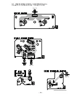
Страница 20: ... 20 SECTION 7 DIAGRAMS Circuit Boards Location TABLE SENSOR board DISC SENSOR R board DISC SENSOR S board AUDIO board BD board SW board MOTOR board POWER SW board LED board MAIN board DISPLAY board ...

Страница 21: ...ur la sécurité Ne les remplacer que par une piéce portant le numéro spécifié U B Line V B Line H adjustment for repair Voltages and waveforms are dc with respect to ground under no signal conditions no mark PLAY Voltages are taken with aVOM Input impedance 10 MΩ Voltage variations may be noted due to normal produc tion tolerances Waveforms are taken with a oscilloscope Voltage variations may be no...

Страница 22: ...E 3 IC101 7 TE PLAY MODE 4 IC102 PCK 5 IC102 XOUT 6 IC102 º 16M 7 IC102 4 2M MAIN Section 1 IC501 XTAL 1 8 Vp p 0 3 0 2 560 mVp p 460 mVp p 6 2 Vp p 230 ns 3 6 Vp p 16 9344 MHz 5 4 Vp p 4 2 MHz 4 4 Vp p 10 MHz 6 2 Vp p 16 MHz DIAPLAY Section 1 IC901 OSC0 2 3 Vp p 480 ns ...

Страница 23: ...OFF TES HFL 35 31 DOUT MUTEL 45 44 XOUT 27 CONT4 S101 LIMIT IN XIN V P CLV CLV RFSM X101 16 9344MHz LASER DIODE TRACKING COIL DRIVE 22 19 20 FOCUS TRACKING COIL DRIVE IC103 1 2 FOCUS COIL DRIVE 15 15 16 27 17 18 2 AXIS DEVICE TRACKING COIL FOCUS COIL T F T F SLED SERVO IC101 2 2 SLED SPINDLE MOTOR DRIVE IC103 2 2 30 31 29 10 SLED MOTOR DRIVE 7 8 M M102 SLED MOTOR SPINDLE MOTOR DRIVE MUTE 3 2 5 6 M...

Страница 24: ...D201 D202 RECT D203 D204 5V REGULATOR IC201 2 2 7 1 7V REGULATOR IC202 3 1 5V REGULATOR IC203 2 2 3 1 30V REGULATOR Q201 DISC SENSOR D51 MUTING CONTROL SWITCH Q383 LOUT RST MUTEL DOUT XMODE SCLK SRDT DQSY RWC WRQ DRF COIN SQOUT CQCK SL SL XMODE ICSW LDOUT LDIN TBLL TBLR ZMUTE SCLK SRDT DQSY RWC WRQ DRF COIN SQOUT CQCK SL SL TGL TGL RESET FLLT FLCK FLDT LEDL HHOUT D SENS DOORSW OPEN CLOSE JOG1 JOG2...

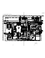
Страница 25: ...RINTED WIRING BOARD BD Section See page 20 for Circuit Boards Location See page 21 for Note Semiconductor Location Ref No Location D151 D 1 IC101 D 3 IC102 B 3 IC103 B 1 IC104 B 2 Q101 B 4 Q102 B 4 Q103 E 1 Page 35 Page 36 ...

Страница 26: ...n See page 21 for Note no mark PLAY Signal path J CD c digital out 29 30 The components identified by mark or dotted line with mark are critical for safety Replace only with part number specified Les composants identifiés par une marque sont critiques pour la sécurité Ne les remplacer que par une piéce portant le numéro spécifié Page 38 Page 38 ...

Страница 27: ...page 21 for Note IC701 A 8 Q301 B 7 Q302 B 7 Q303 A 6 Q331 C 7 Q401 B 6 Q402 B 7 Q403 B 6 Q431 C 7 Q701 A 7 Ref No Location Ref No Location D201 C 5 D202 C 5 D203 C 5 D204 D 5 D205 B 5 D701 A 7 IC301 B 8 IC302 B 7 IC401 C 7 IC402 C 6 Semiconductor Location 32 31 Page 36 Page 35 Page 36 Page 44 ...

Страница 28: ...c digital out The components identified by mark or dotted line with mark are critical for safety Replace only with part number specified Les composants identifiés par une marque sont critiques pour la sécurité Ne les remplacer que par une piéce portant le numéro spécifié Page 45 Page 38 Page 38 Page 38 ...

Страница 29: ...cation D206 E 2 D207 D 2 D210 C 1 D211 C 1 D212 C 1 D304 E 1 D382 D 1 D404 E 1 D501 C 4 IC201 C 2 IC202 B 1 IC203 A 4 IC501 B 4 IC502 D 4 IC601 E 4 Q201 E 2 Q304 E 1 Q305 A 1 Q380 C 1 Q381 D 1 Q382 D 1 Q383 E 1 Q404 E 1 Q405 B 1 Q481 C 1 Q501 D 3 Q502 D 3 35 36 Page 43 Page 32 Page 28 Page 28 Page 32 Page 32 Page 43 Page 43 Page 39 Page 44 ...

Страница 30: ...page 22 for Waveform See page 47 for IC Block Diagrams See page 53 for IC Pin Function Description See page 21 for Note 37 38 no mark PLAY Signal path J CD c digital out Page 45 Page 45 Page 45 Page 41 Page 45 Page 30 Page 30 Page 33 Page 33 Page 33 ...

Страница 31: ...ds Location See page 21 for Note 39 40 Semiconductor Location DISPLAY Board D901 D 7 D902 D 6 D903 D 4 D904 D 5 D905 D 5 D906 D 4 D907 D 4 D908 D 3 Ref No Location Ref No Location IC901 B 5 IC902 A 1 IC903 C 7 Q901 C 4 Q902 E 6 Q903 D 6 Q904 D 5 Q905 D 6 Page 40 Page 39 Page 36 ...

Страница 32: ...CDP CX57 41 42 7 9 SCHEMATIC DIAGRAM PANEL Section See page 22 for Waveform See page 48 for IC Block Diagram See page 21 for Note Page 38 ...

Страница 33: ... 43 7 10 PRINTED WIRING BOARDS SENSOR MOTOR Section See page 20 for Circuit Boards Location See page 21 for Note Page 36 Page 36 Page 35 ...

Страница 34: ... 44 Page 31 Page 36 ...

Страница 35: ... 45 7 11 SCHEMATIC DIAGRAM SENSOR MOTOR Section See page 21 for Note CDP CX57 Page 33 Page 37 Page 37 Page 38 Page 37 ...

Страница 36: ... XVDD MUTER RVDD RCHO RVSS LVSS LCHO LVDD MUTEL N C TEST4 TAI PDO VVSS ISET VVDD FR VSS EFMO EFMIN TEST2 CLV CLV V P HFL TES SLICE LEVEL CONTROL µCOM INTERFACE XTAL TIMING GENERATOR 2K x 8BIT RAM RAM ADDRESS GENERATOR MUTE SERVO COMMANDER CLV DIGITAL SERVO DIGITAL ATTENUATOR OVERSAMPLING DIGITAL FILTER 1BIT DAC L P F DIGITAL OUT GENERAL PORT VCO CLOCK OSCILLATION CLOCK CONTROL SYNCRONOUS DETECTION...

Страница 37: ...L DRIVER BTL DRIVER LEVEL SHIFT LEVEL SHIFT REGULATOR RESET Vcc 1 2 3 4 5 7 6 V IN EN GND CDEL CN RES V OUT REFERENCE VOLTAGE OVER HEAT PROTECTION OVER CURRENT LIMITTER ON OFF RESET GEN ERROR AMP 3 6 7 2 5 1 4 9 8 10 ON OFF AMP V REF AMP RESET VOMUTE CD VIN VO RES CN GND EN VID VOD IC104 LC89170M 1 2 3 4 5 6 7 14 13 12 11 10 9 8 TIMING SYNCHRONIZATION SIGNAL PROTECTION 32 WORD X 8 BIT DUAL PORT RA...

Страница 38: ...REF VREG VCC OUT1 OUT1 18 17 16 15 1 2 3 4 5 6 7 8 9 14 13 12 11 10 24 0 D R CK 23 0 D R CK 22 0 D R CK 21 0 D R CK 20 0 D R CK 19 0 D R CK 18 0 D R CK 17 0 D R CK 16 0 D R CK 15 0 D R CK 14 0 D R CK 13 4 5 6 7 8 9 10 11 12 0 D R CK 1 D R CK 1 D R CK 1 D R CK 1 D R CK 1 D R CK 1 D R CK 1 D R CK 1 D R CK 1 D R CK 1 D R CK 1 D R CK 1 D R CK D 1 R CK D 1 0 0 R CK D R CK D R CK 1 2 3 D 1 R CK D 1 0 0 ...

Страница 39: ...ocusing phase compensation constant between FD pin and FA pin ª pins 19 FA I Creates a focusing phase compensation constant between FA pin and FE pin º pins 20 FE O Focus error signal output terminal 21 FE I Focus error signal invert signal input terminal 22 AGND Ground terminal analog system 23 SP O Single end output of the CV pin º and CV pin ª pins signal 24 SPI I Spindle amplifier input termin...

Страница 40: ...and serial clock signal input from the system controller IC501 52 DAT I Command serial data input from the system controller IC501 53 CE I Command chip enable signal input from the system controller IC501 54 DRF O Focus OK signal output to the system controller IC501 L NG H OK 55 FSS I FSS Focus Search Select is a switching terminal for the focus search mode search search for a reference voltage N...

Страница 41: ...ock monitor output terminal 4 3218 MHz when phase is locked 22 FSEQ O Sync signal detection output terminal H when a sync signal detected from the EFM signal and that generated internally coincide 23 VDD Power supply terminal 5V digital system 24 CONT1 I Guard frame sync input terminal 25 CONT2 I Sled servo on off control signal input terminal 26 CONT3 O Sled servo drive control signal output term...

Страница 42: ...bcode Q synchronizing signal output to the system controller IC501 54 RWC I Command chip enable signal input from the system controller IC501 schmitt input 55 SQOUT O Subcode Q data output to the system controller IC501 56 COIN I Command serial data input from the system controller IC501 57 CQCK I Command serial clock signal input from the system controller IC501 schmitt input Fetching clock input...

Страница 43: ...d for the BD section reset H active 30 RESET I System reset signal input from the reset signal generator IC203 L reset For several hundreds msec after the power supply rises L is input then it changes to H 31 EXTAL I Main system clock input terminal 10 MHz 32 XTAL O Main system clock output terminal 10 MHz 33 VSS Ground terminal 34 TX O Sub system clock output terminal Not used open 35 TEX I Sub s...

Страница 44: ...ive 59 SL O Sled feeding signal internal direction output to the RF amplifier IC101 H active 60 DQSY I Serial data synchronizing signal input from the CD text decoder IC104 L active 61 XMODE O Reset signal output to the CD text decoder IC104 H reset 62 T SENS1 I Disc table flag detect sensor IC51 input terminal 63 T SENS2 I Disc table flag detect sensor IC52 input terminal 64 T SENS3 I Disc table ...

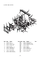
Страница 45: ... views are not supplied Hardware mark list and accessories and packing materials are given in the last of the electrical parts list NOTE XX and X mean standardized parts so they may have some difference from the original one Color Indication of Appearance Parts Example KNOB BALANCE WHITE RED Parts Color Cabinet s Color Ref No Part No Description Remark Ref No Part No Description Remark 1 CASE SECT...

Страница 46: ... 008 600 01 EMBLEM 5 AR SONY 58 4 997 062 11 PANEL FRONT 59 4 991 156 01 INDICATOR POWER 60 4 991 152 11 BUTTON POWER 61 1 668 578 11 POWER SW BOARD 62 4 951 620 01 SCREW 2 6X8 BVTP 63 4 933 134 61 SCREW PTPWH M2 6X6 64 X 4949 357 1 BUTTON MAIN ASSY 65 4 996 359 11 BUTTON BLOCK 66 A 4724 009 A DISPLAY BOARD COMPLETE 67 1 773 140 11 WIRE FLAT TYPE 19 CORE 68 4 978 398 21 CUSHION 69 3 354 963 21 DAM...

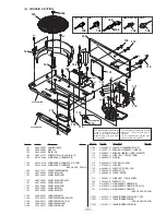
Страница 47: ...1 CORD POWER AEP AED SP 108 1 590 926 11 CORD POWER US CND 108 1 696 845 11 CORD POWER AUS 108 1 751 529 11 CORD POWER UK 109 1 569 007 11 ADAPTOR CONVERSION 2P E 110 3 703 571 11 BUSHING S FBS002 CORD E 110 4 966 267 11 BUSHING FBS001 CORD EXCEPT E 111 1 782 465 11 WIRE FLAT TYPE 16 CORE 112 4 990 029 01 RING B 113 X 4946 543 2 FOOT SMALL ASSY 114 4 978 398 21 CUSHION 115 4 990 895 01 SUPPORT P T...

Страница 48: ...020 1 LEVER LOADING ASSY 309 4 988 438 01 SPRING LEVER TENSION 310 4 988 437 01 SPRING HOLDER TORSION 311 4 988 416 01 BASE LOADING 312 4 988 419 01 HOLDER B DISC 313 4 992 069 01 SCREW PTPWH M2 DIA 7 314 4 988 454 01 COVER LEVER 315 4 988 421 01 HOLDER MAGNET 316 A 4672 522 A MAGNET ASSY 317 4 960 633 11 YOKE MAGNET 318 4 999 139 01 PULLEY B 319 4 976 473 01 HOLDER LED S 320 4 988 431 01 ROLLER D...

Страница 49: ...M62 351 1 663 971 11 TABLE SENSOR BOARD 352 4 988 414 01 BELT 353 4 988 423 01 GEAR A LOADING 354 4 988 425 01 PULLEY 355 4 988 424 01 GEAR TABLE 356 4 988 432 01 GEAR B LOADING 357 4 988 426 01 BASE CDM 358 1 663 972 11 DISC SENSOR R BOARD 359 1 663 974 11 MOTOR BOARD 360 4 990 669 01 HOLDER SENSOR M61 X 4948 434 1 MOTOR ASSY LOADING M62 X 4948 434 1 MOTOR ASSY TABLE ...

Страница 50: ... 006 A BD BOARD COMPLETE 406 4 992 054 01 RUBBER VIBRATION PROOF 407 4 996 243 01 SCREW M2 PSW 408 1 777 874 11 WIRE FLAT YTPE 16 CORE 409 X 2646 108 2 TURN TABLE ASSY AU F M101 X 2646 110 2 T T CHASSIS ASSY MG F SPINDLE M102 X 2625 769 1 MOTOR GEAR ASSY MB RP SLED The components identified by mark or dotted line with mark are critical for safety Replace only with part num ber specified Les compos...

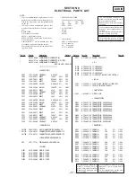
Страница 51: ...ECT 22uF 20 50V C701 1 104 665 11 ELECT 100uF 20 10V C702 1 161 494 00 CERAMIC 0 022uF 25V C704 1 162 282 31 CERAMIC 100PF 10 50V C708 1 161 494 00 CERAMIC 0 022uF 25V CONNECTOR CN201 1 580 230 11 PIN CONNECTOR PC BOARD 2P CN701 1 766 955 11 CONNECTOR BOARD TO BOARD 11P CN703 1 778 981 11 CONNECTOR BOARD TO BOARD 13P GROUND TERMINAL BOARD CP2 1 537 771 21 TERMINAL BOARD GROUND DIODE D201 8 719 200...

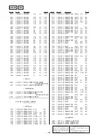
Страница 52: ... 16V C109 1 164 161 11 CERAMIC CHIP 0 0022uF 10 100V C110 1 163 037 11 CERAMIC CHIP 0 022uF 10 25V C111 1 163 989 11 CERAMIC CHIP 0 033uF 10 25V C112 1 163 009 11 CERAMIC CHIP 0 001uF 10 50V C113 1 164 492 11 CERAMIC CHIP 0 15uF 10 16V C114 1 164 492 11 CERAMIC CHIP 0 15uF 10 16V C115 1 164 232 11 CERAMIC CHIP 0 01uF 50V C116 1 164 232 11 CERAMIC CHIP 0 01uF 50V C117 1 163 001 11 CERAMIC CHIP 220P...

Страница 53: ... R128 1 216 077 00 METAL CHIP 15K 5 1 10W R129 1 216 069 00 METAL CHIP 6 8K 5 1 10W R130 1 216 113 00 METAL CHIP 470K 5 1 10W R131 1 216 113 00 METAL CHIP 470K 5 1 10W R132 1 216 065 00 RES CHIP 4 7K 5 1 10W R133 1 216 113 00 METAL CHIP 470K 5 1 10W R134 1 216 113 00 METAL CHIP 470K 5 1 10W R135 1 216 065 00 RES CHIP 4 7K 5 1 10W R136 1 216 073 00 METAL CHIP 10K 5 1 10W R137 1 216 009 00 METAL CHI...

Страница 54: ...CARBON 1K 5 1 4W R909 1 249 419 11 CARBON 1 5K 5 1 4W R910 1 249 421 11 CARBON 2 2K 5 1 4W R911 1 247 843 11 CARBON 3 3K 5 1 4W R912 1 249 427 11 CARBON 6 8K 5 1 4W R913 1 249 431 11 CARBON 15K 5 1 4W R914 1 249 415 11 CARBON 680 5 1 4W R915 1 249 417 11 CARBON 1K 5 1 4W R916 1 249 419 11 CARBON 1 5K 5 1 4W R917 1 249 421 11 CARBON 2 2K 5 1 4W R918 1 247 843 11 CARBON 3 3K 5 1 4W R930 1 247 843 11...

Страница 55: ...8 11 PIN CONNECTOR 3P CN603 1 568 955 11 PIN CONNECTOR 6P CN702 1 770 730 11 CONNECTOR BOARD TO BOARD 11P CN704 1 778 982 11 CONNECTOR BOARD TO BOARD 13P CN801 1 506 468 11 PIN CONNECTOR 3P DIODE D206 8 719 921 54 DIODE MTZJ 6 2B D207 8 719 982 22 DIODE MTZJ 30D D210 8 719 991 33 DIODE 1SS133T 77 D211 8 719 921 42 DIODE MTZJ 5 1A D212 8 719 991 33 DIODE 1SS133T 77 D304 8 719 991 33 DIODE 1SS133T 7...

Страница 56: ...LPDJA STANDBY D910 8 719 057 97 LED SEL5923A TP15 MEGA CONTROL D911 8 719 057 97 LED SEL5923A TP15 MEGA CONTROL TRANSISTOR Q906 8 729 900 80 TRANSISTOR DTC114ES Q907 8 729 119 76 TRANSISTOR 2SA1175 HFE RESISTOR R919 1 249 415 11 CARBON 680 5 1 4W R920 1 249 417 11 CARBON 1K 5 1 4W R921 1 249 419 11 CARBON 1 5K 5 1 4W R946 1 249 407 11 CARBON 150 5 1 4W R947 1 249 429 11 CARBON 10K 5 1 4W R948 1 24...

Страница 57: ...AN ITALIAN SPANISH DUTCH SWEDISH PORTUGUESE CHINESE CND AEP E SP 3 862 557 11 MANUAL INSTRUCTION ENGLISH EXCEP AED 3 862 557 21 MANUAL INSTRUCTION FRENCH SPANISH CHINESE CND AEP E SP 3 862 557 31 MANUAL INSTRUCTION GERMAN DUTCH ITALIAN PORTUGUESE AEP 3 862 557 41 MANUAL INSTRUCTION SWEDISH FINNISH DANISH AED 4 981 643 01 COVER BATTERY for RM DX57 4 991 161 01 LET 50 BOOK 4 991 854 01 LABEL DISC HA...

Страница 58: ... 68 CDP CX57 Sony Corporation Home A V Products Company 9 922 818 11 98D0589 1 Printed in Japan 1998 4 Published by Quality Assurance Dept Shibaura ...

Отзывы: