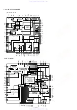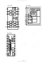
— 41 —
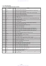
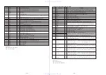
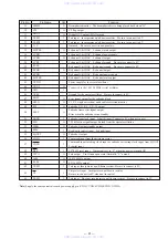
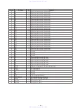
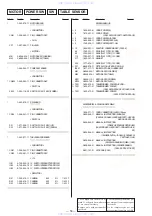
Pin No.
Pin Name
I/O
Function
29
30
31
32
33
34
35
36
37
38
39
40
41
42
43
44
45
46
47
48
49
50
51
52
53
54
55
56
57
58
O
O
O
I
I
–
O
–
O
–
–
O
–
O
–
O
I
–
O
O
O
O
I
O
O
I
O
I
I
I
O
O
O
I
I
Deemphasis monitor
The deemphasis disc is being played back when “H”
C2 flag output
Digital OUT output (EIAJ format)
Test input
Incorporates a pull-down resistor
Be sure to connect to 0V
Test input
Incorporates a pull-down resistor
Be sure to connect to 0V
Not used
Be sure to use it in an open state
L channel 1-bit DAC
L channel mute output
L channel 1-bit DAC
L channel power supply
L channel 1-bit DAC
L channel output
L channel 1-bit DAC
L channel ground
Be sure to connect to 0V
R channel 1-bit DAC
R channel ground
Be sure to connect to 0V
R channel 1-bit DAC
R channel output
R channel 1-bit DAC
R channel power supply
R channel 1-bit DAC
R channel mute output
Power supply for the crystal oscillator
Connected to the 16.9344 MHz crystal oscillator
Ground for the crystal oscillator
Be sure to connect to 0V
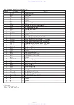
Sync signal output for the subcode block
C1, C2, single correction, and double correction monitor
Subcode P, Q, R, S, T, U, W output
Subcode frame sync signal output
Rises when the subcode is in a standby
Subcode read clock input
Schmidt input (Connect to 0V when not in use)
7.35 kHz sync signal output divided from the crystal oscillation
Subcode Q output standby output
Read/write control input
Schmidt input
Subcode Q output
Command input from the microprocessor
Command input fetching clock input or subcode extracting clock input from SQOUT
Schmidt input
LC78622 reset input
Temporarily set to “L” when the power is turned ON
Test output
Use it in an open state (Normally, “L” output)
16.9344 MHz output
4.2336 MHz output
Test input. Incorporates a pull-down resistor. Be sure to connect to 0V
Chip select input
Incorporates a pull-down resistor
Be sure to connect to 0V when not in control
Test input
Does not incorporates a pull-down resistor
Be sure to connect to 0V
EMPH
C2F
DOUT
TEST3
TEST4
N. C.
MUTEL
LVDD
LCHO
LVSS
RVSS
RCHO
RVDD
MUTER
XVDD
XOUT
XIN
XVSS
SBSY
EFLG
PW
SFSY
SBCK
FSX
WRQ
RWC
SQOUT
COIN
CQCK
RES
I
Note) Supply the same potential to each power supply pin (VDD, VVDD, LVDD, RVDD, XVDD).
www. xiaoyu163. com
QQ 376315150
9
9
2
8
9
4
2
9
8
TEL 13942296513
9
9
2
8
9
4
2
9
8
0
5
1
5
1
3
6
7
3
Q
Q
TEL 13942296513 QQ 376315150 892498299
TEL 13942296513 QQ 376315150 892498299

