


SH79F3283
86
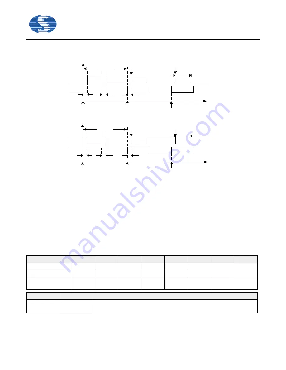
8.3.6 Dead time
SH79F3283 provides dead time function on-chip.
When PWM0S = 0, the dead time is generated as below.
dead time
dead time
PWM0x
PWM01x
PWM0S=0
duty cycle
dead time
period
Reload
PWM Enable
PWM int
Reload
PWM int
x=A,B,C
x=A,B,C
When PWM0S = 1, the dead time is generated as below.
dead time
dead time
PWM0x
PWM01x
PWM0S=1
duty cycle
dead time
period
Reload
PWM Enable
PWM int
Reload
PWM int
x=A,B,C
x=A,B,C
By writing PWM0 dead time control register, a dead time can be generated between PWM0x (x = A, B, C) and PWM01x (x =
A, B, C).
PWM01x (x = A, B, C) has the same period as PWM0x (x = A, B, C)
Note:
(1) The dead time must be set before PWM output enable. Otherwise, dead time will not change. So in order to change dead
time, please disable PWM output first (While PWMLO is #55H), then change the dead time, enable PWM output. Finally,
change the data in PWMLO not equal to #55H in order to make sure the PWM registers would not be changed by noise.
(2) In order to generate dead time, please make sure that (PWM0x Period-PWM0x Duty) > 2 X PWM01x dead time control.
Otherwise the output of PWM01x is high level when PWMS = 1 or GND when PWMS = 0.
(3) PWMDT is to used to control Dead Time, the step value is fixed oscillator clock time, but period and duty value is refer to
TnCK2-0. 2 oscillator clocks at least.
(4) If dead time is needed, any time when PWM is disabled, before enable PWM again, dead time register must be clear to 0
at first, and then set the proper value.
Table 8.20
PWM0 Dead Time Control Register
D1H
Bit7
Bit6
Bit5
Bit4
Bit3
Bit2
Bit1
Bit0
PWM0DT
DT0.7
DT0.6
DT0.5
DT0.4
DT0.3
DT0.2
DT0.1
DT0.0
R/W
R/W
R/W
R/W
R/W
R/W
R/W
R/W
R/W
Reset Value
(POR/WDT/LVR/PIN)
0
0
0
0
0
0
0
0
Bit Number
Bit Mnemonic
Description
7-0
DT0[7:0]
12 bit PWM0 dead time control
The dead time period = (DT0.7 - DT0.0) X t
OSC


