Smart Machine Smart Decision
SIM800_Hardware Design_V1.10
14
2018-08-13
3.
Package Information
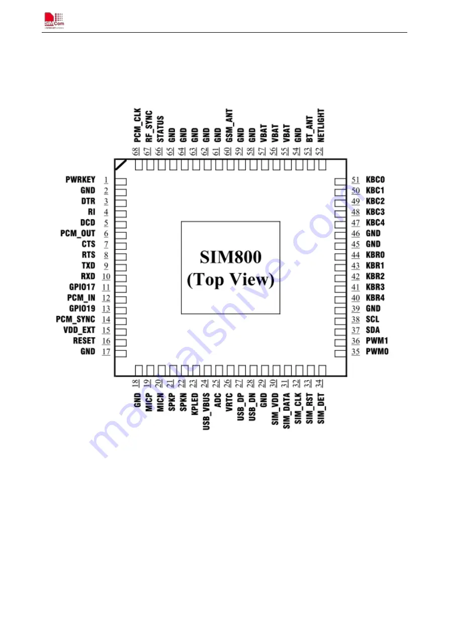
3.1.
Pin Out Diagram
Figure 2: SIM800 pin out diagram (Top view)
Страница 1: ...SIM800_Hardware Design_V1 10...
Страница 2: ...customer s possession Furthermore system validation of this product designed by SIMCom within a larger electronic system remains the responsibility of the customer or the customer s system integrator...
Страница 3: ...Mode 26 4 3 2 Sleep Mode AT CSCLK 1 27 4 3 3 Wake Up SIM800 from Sleep Mode AT CSCLK 1 27 4 4 RTC Backup 27 4 5 Serial Port and USB Interface 28 4 5 1 Function of Serial Port 29 4 5 2 Serial Port 29 4...
Страница 4: ...eliability and Radio Characteristics 53 6 1 Absolute Maximum Ratings 53 6 2 Recommended Operating Conditions 53 6 3 Digital Interface Characteristics 53 6 4 SIM Card Interface Characteristics 54 6 5 S...
Страница 5: ...LE 19 PCM SPECIFICATION 41 TABLE 20 PIN DEFINITION OF THE KEYPAD INTERFACE 43 TABLE 21 PIN DEFINITION OF THE I2C 44 TABLE 22 PIN DEFINITION OF THE GPIO 44 TABLE 23 PIN DEFINITION OF THE ADC 45 TABLE 2...
Страница 6: ...46 CONDUCTED RF RECEIVE SENSITIVITY 57 TABLE 47 OPERATING FREQUENCIES 58 TABLE 48 MOISTURE CLASSIFICATION LEVEL AND FLOOR LIFE 60 TABLE 49 BAKING REQUIREMENTS 60 TABLE 50 TRAY SIZE 61 TABLE 51 SMALL...
Страница 7: ...30 FIGURE 21 ISOLATION CIRCUIT BY DIODES 30 FIGURE 22 TX LEVEL CONVERTING BY TRANSISTOR 31 FIGURE 23 RX LEVEL CONVERTING BY TRANSISTOR 31 FIGURE 24 USB REFERENCE CIRCUIT 32 FIGURE 25 CONNECTION FOR SO...
Страница 8: ...NG CIRCUIT 49 FIGURE 48 BLUETOOTH ANTENNA MATCHING CIRCUIT 50 FIGURE 49 RECOMMENDED PCB LAYOUT 52 FIGURE 50 TOP AND BOTTOM VIEW OF SIM800 59 FIGURE 51 TYPICAL SOLDER REFLOW PROFILE 59 FIGURE 52 PACKAG...
Страница 9: ...onggang 2014 07 18 1 06 Update figure 12 and 13 timing of VDD_EXT changed Update the baudrate that SIM800 supports Rename some pin name to follow the SIMCom naming rules Uptade table 6 table9 Add GPIO...
Страница 10: ...ads One full function UART port and can be configured to two independent serial ports One USB port can be used as debugging and firmware upgrading Audio channels which include a microphone input and a...
Страница 11: ...es Half Rate ETS 06 20 Full Rate ETS 06 10 Enhanced Full Rate ETS 06 50 06 60 06 80 Adaptive multi rate AMR Echo Cancellation Noise Suppression Serial port and USB interface Serial port Full modem int...
Страница 12: ...ion depends on network settings such as DTX off on FR EFR HR hopping sequences antenna GPRS STANDBY Module is ready for GPRS data transfer but no data is currently sent or received In this case power...
Страница 13: ...figure shows a functional diagram of SIM800 GSM baseband engine PMU RF part Antenna interfaces Other interfaces Analog Baseband Digital Baseband Power Management Unit Radio Frequency Power Supply Anal...
Страница 14: ...Smart Machine Smart Decision SIM800_Hardware Design_V1 10 14 2018 08 13 3 Package Information 3 1 Pin Out Diagram Figure 2 SIM800 pin out diagram Top view...
Страница 15: ...itor e g 4 7uF VDD_EXT 15 O 2 8V power output Keep floating if unused GND 2 17 18 29 3 9 45 46 54 5 8 59 61 62 6 3 64 65 Ground GND for VBAT recommend to use 62 63 64 65 pin Power on off PWRKEY 1 I PW...
Страница 16: ...grading Keep floating if unused USB_DP 27 I O USB_DN 28 I O ADC ADC 25 I 10 bit general analog to digital converter Keep floating if unused PWM PWM0 35 O Pulse width modulation multiplex with GPIO Kee...
Страница 17: ...n_V1 10 17 2018 08 13 BT_ANT 53 I O Bluetooth antenna port Impendence must be controlled to 50 RF synchronization RF_SYNC 67 O RF burst synchronous signal Do not pull up Other signal RESET 16 I Reset...
Страница 18: ...Smart Machine Smart Decision SIM800_Hardware Design_V1 10 18 2018 08 13 3 3 Package Dimensions Figure 3 Dimensions of SIM800 Unit mm...
Страница 19: ...Smart Machine Smart Decision SIM800_Hardware Design_V1 10 19 2018 08 13 Figure 4 Recommended PCB footprint outline Unit mm Note Keep copper out of area B and C...
Страница 20: ...33pF and 10pF capacitors can effectively eliminate the high frequency interference A 5 1V 500mW Zener diode is strongly recommended the diode can prevent chip from damaging by the voltage surge These...
Страница 21: ...596 ADJ 100uH MBR360 L101 C101 C102 D102 C103 R102 R101 FB101 330uF VBAT 2 2K 1K 100uF 1uF C104 100nF DC INPUT PWR_CTRL GND On Off c Figure 7 Reference circuit of the DC DC power supply The single 3 7...
Страница 22: ...voltage drops below 3 4V the module may be shut down automatically The PCB traces from the VBAT pins to the power supply must be wide enough at least 80mil to decrease voltage drops in the transmit bu...
Страница 23: ...D_EXT STATUS T 1 2s Serial Port T 1 4s Figure 12 Timing of power on module When power on procedure is completed SIM800 will send following URC to indicate that the module is ready to operate at fixed...
Страница 24: ...n time exceeds 33 seconds will course the module power up This procedure makes the module log off from the network and allows the software to enter into a secure state to save data before completely s...
Страница 25: ...TC is still active Power off mode can also be indicated by STATUS pin which is low level at this time 4 2 3 Reset Function SIM800 also have a RESET pin used to reset the module This function is used a...
Страница 26: ...n When SIM800 is in sleep mode and minimum function mode the current of module is the lowest 4 3 1 Function Mode There are three function modes which could be set by the AT command AT CFUN fun The com...
Страница 27: ...ule after module power on 4 3 3 Wake Up SIM800 from Sleep Mode AT CSCLK 1 When SIM800 is in sleep mode AT CSCLK 1 the following methods can wake up the module Pull down DTR pin The serial port will be...
Страница 28: ...RTC refer to table 44 4 5 Serial Port and USB Interface SIM800 provides one unbalanced asynchronous serial port The module is designed as a DCE Data Communication Equipment The following figure shows...
Страница 29: ...rates 1200 2400 4800 9600 19200 38400 57600 and 115200bps The default setting is autobauding Autobauding allows SIM800 to automatically detect the baud rate of the host device Pay more attention to t...
Страница 30: ...reference circuits are recommended If the voltage is 3 0V please change the resistors in the following figure from 5 6K to 14K 1K 5 6K RXD TXD RTS CTS GPIO GPIO EINT DTE 3 3V 5 6K 5 6K 1K 1K 1K 1K 1K...
Страница 31: ...nce circuits VDD_EXT 4 7K 47K UART1_TXD 4 7K Module VDD_EXT RXD VDD DTE Figure 22 TX level converting by transistor VDD_EXT 4 7K 47K 4 7K DTE UART1_RXD Module VDD_EXT TXD VDD Figure 23 RX level conver...
Страница 32: ...USB and UART interfaces can be used for firmware upgrade If customer upgrading firmware via the USB port SIM800 must be powered first then connect USB_VBUS USB_DP USB_DN and GND to PC There is no nee...
Страница 33: ...ur the pin will be changed to high 1 Establish the call 2 Hang up the call Data call The pin is changed to low When any of the following events occur the pin will be changed to high 1 Establish the ca...
Страница 34: ...in high Please refer to the following figure HIGH LOW Idle Ring Establish the call Hang up the call Idle RI Figure 29 RI behaviour as a caller 4 7 Audio Interfaces SIM800 provides one analog input whi...
Страница 35: ...gnals have to be layout according to differential signal layout rules as shown in following figures 4 7 1 Speaker Interfaces Configuration SPKP Close to speaker ESD ESD 10pF 33pF 33pF 33pF Module SPKN...
Страница 36: ...develop this filter solution according to field test result GSM antenna is the key coupling interfering source of TDD noise Pay attention to the layout of audio lines which should be far away from RF...
Страница 37: ...nce circuit of the 8 pin SIM card holder is illustrated in the following figure Module SMF12C VSIM SIM_CLK SIM_DATA SIM_RST SIM_PRE PRESENCE 51R 1uF MOLEX 91228 SIM Card 22PF 4 7K VDD_EXT VCC GND RST...
Страница 38: ...while designing Make sure that SIM card holder should far away from GSM antenna while in PCB layout SIM traces should keep away from RF lines VBAT and high speed signal lines The traces should be as...
Страница 39: ...scription C1 SIM_VDD SIM card power supply C2 SIM_RST SIM card reset C3 SIM_CLK SIM card clock C4 GND Connect to GND C5 GND Connect to GND C6 VPP Not connect C7 SIM_DATA SIM card data I O C8 SIM_DET D...
Страница 40: ...Signal Description C1 SIM_VDD SIM card power supply C2 SIM_RST SIM card reset C3 SIM_CLK SIM card clock C5 GND Connect to GND C6 VPP Not connect C7 SIM_DATA SIM card data I O 4 10 PCM Interface SIM800...
Страница 41: ...PCMSYNC PCMOUT PCMCLK GND GND PCM_IN PCM_OUT PCM_SYNC PCM_CLK Figure 36 PCM reference circuit 4 11 Keypad Interface SIM800 consists of 5 keypad column outputs and 5 keypad row inputs and it can suppor...
Страница 42: ...d KBCs and KBRs as GPIO for details please see the document 1 Module supports a new keypad connection it can support 5 5 2 amount 50 keypads meet full keyboard demand and the connection diagram is as...
Страница 43: ...on same KBC and KBR when implement the extended keypad design The following figure is an example to explain this situation CTRL and A can not be recognized if the two buttons were pressed at the same...
Страница 44: ...e drive write and I O configuration Table 21 Pin definition of the I2C Note I2C has been pulled up to 2 8V via 4 7K inside 4 13 General Purpose Input Output GPIO SIM800 provides 2 GPIO pins The output...
Страница 45: ...able 24 ADC specification Parameter Min Typ Max Unit Voltage range 0 2 8 V ADC Resolution 10 bits Sampling rate 1 0833 MHz ADC precision 10 30 mV Note the voltage should less than 2 8V or the ADC may...
Страница 46: ...le 26 PWM output characteristics Parameter Min Typ Max Unit Working voltage 2 5 2 8 2 9 V Working current 4 16 mA Note PWM pin must keep low when module in the boot process Table 27 PWM multiplex func...
Страница 47: ...BAT 4 7K 47K R Figure 43 Reference circuit of NETLIGHT 4 17 Operating Status Indication The STATUS pin indicates the operating status of module The pin output high when module power on output is low w...
Страница 48: ...the transmit burst Table 33 Definition of the RF_SYNC pin Note Do not pull up RF_SYNC The timing of the synchronization signal is shown in the following figure High level of the RF_SYNC signal indica...
Страница 49: ...an inductor for ESD protection The GSM antenna must be matched properly to achieve the best performance so the matching circuit is necessary For the purpose of static electricity we recommend to add D...
Страница 50: ...tenna interface named BT_ANT to connect a Bluetooth antenna The Bluetooth antenna must be matched properly to achieve best performance so the matching circuit is necessary the connection is recommende...
Страница 51: ...ces The RF connector is used for conducted test so keep it as close to the GSM_ANT pin as possible Antenna matching circuit should be closed to the antenna Keep the RF traces as 50 The RF traces shoul...
Страница 52: ...o should far away from antenna and power and it is recommended to surround audio traces by ground And do not rout audio trace and VBAT trace parallel 5 2 5 Others It s better to trace signal lines of...
Страница 53: ...parameters are for digital interface pins such as keypad GPIO I2C UART LCD and PCM 6 2 Recommended Operating Conditions Table 36 Recommended operating conditions Symbol Parameter Min Typ Max Unit VBA...
Страница 54: ...7 V VOL Low level output voltage 0 36 V 0 4 V 6 5 SIM_VDD Characteristics Table 39 SIM_VDD characteristics Symbol Parameter Min Typ Max Unit VO Output voltage 3 0 V 1 8 IO Output current 10 mA 6 6 VDD...
Страница 55: ...1 2 1 3 2 0 mA Idle mode AT CFUN 1 EGSM900 22 1 mA Voice call PCL 5 GSM850 EGSM900 DCS1800 PCS1900 204 8 203 9 133 1 137 9 mA Data mode GPRS 1Rx 4Tx GSM850 EGSM900 DCS1800 PCS1900 450 9 457 3 281 8 2...
Страница 56: ...discharge VBAT 5KV 10KV GND 5KV 10KV RXD TXD 4KV 8KV GSM_ANT 5KV 10KV SPKP SPKN MICP MICN 4KV 8KV PWRKEY 4KV 8KV 6 10 Radio Characteristics The following table shows the module conducted output power...
Страница 57: ...11 8 4 5 12 6 4 5 13 4 4 5 14 2 5 6 15 0 5 6 6 11 Module RF Receive Sensitivity The following table shows the SIM800 conducted receive sensitivity it is tested under static condition Table 46 Conduct...
Страница 58: ...V1 10 58 2018 08 13 Table 47 Operating frequencies Frequency Receive Transmit Channel GSM850 869 894MHz 824 849MHz 128 251 EGSM900 925 960MHz 880 915MHz 0 124 975 1023 DCS1800 1805 1880MHz 1710 1785MH...
Страница 59: ...Manufacturing 7 1 Top and Bottom View of SIM800 Figure 50 Top and Bottom View of SIM800 7 2 Typical Solder Reflow Profile Figure 51 Typical Solder Reflow Profile Note Please refer to Module secondary...
Страница 60: ...If the vacuum package is not open for 6 months or longer than the packing date baking is also recommended before re flow soldering 2 For product handling storage processing IPC JEDEC J STD 033 must b...
Страница 61: ...ision SIM800_Hardware Design_V1 10 61 2018 08 13 8 Packaging Module support tray packaging Figure 52 packaging diagram Module tray drawing Figure 53 Tray drawing Table 50 Tray size Length 3mm Width 3m...
Страница 62: ...l carton drawing Figure 54 Small carton drawing Table 51 Small Carton size Length 10mm Width 10mm Height 10mm Number 270 180 120 20 20 400 Big carton drawing Figure 55 Big carton drawing Table 52 Big...
Страница 63: ...ice SMS and Cell Broadcast Service CBS 6 GSM 11 14 Digital cellular telecommunications system Phase 2 Specification of the SIM Application Toolkit for the Subscriber Identity Module Mobile Equipment S...
Страница 64: ...Rate GPRS General Packet Radio Service GSM Global Standard for Mobile Communications HR Half Rate IMEI International Mobile Equipment Identity Li ion Lithium Ion MO Mobile Originated MS Mobile Statio...
Страница 65: ...USSD Unstructured Supplementary Service Data VSWR Voltage Standing Wave Ratio Phonebook abbreviations FD SIM fix dialing phonebook LD SIM last dialing phonebook list of numbers most recently dialed MC...
Страница 66: ...e a safety hazard Your cellular terminal or mobile receives and transmits radio frequency energy while switched on RF interference can occur if it is used close to TV sets radios computers or other el...
Страница 67: ..._V1 10 67 2018 08 13 Contact us Shanghai SIMCom Wireless Solutions Ltd Address Building B No 633 Jinzhong Road Changning District Shanghai P R China 200335 Tel 86 21 3157 5100 3157 5200 Email simcom s...