background image

PC-UM10M

XE-A402   SPECIFICATIONS

– 2 –

The mode switch has these settings:

OFF:

This mode locks all register operations. (AC power turns off.)
No change occurs to register data.

OP X/Z: To take individual clerk X or Z reports, and to take flash

reports.

It can be used to toggle receipt state “ON” and “OFF” by press-

ing he [RCP/PO] key.

REG:

For entering sales.

PGM:

To program various items.

VOID:

Enters into the void mode. This mode allows correction after
finalizing a transaction.

MGR:

For manager’s entries. The manager can use this mode for an
override entry.

X1/Z1: To take the X/Z report for various daily totals.

X2/Z2: To take the X/Z report for periodic (weekly or monthly) consoli-

dation.

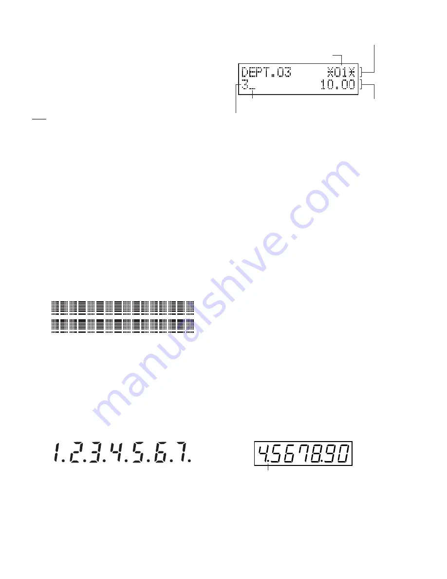
5. DISPLAY

5-1. OPERATOR DISPLAY

Display device

: LCD

Number of line

: 2 line

Number of positions : 16 positions

Color of display

: Yellow / Green

Character form

: Dot matrix

Character size

: 14.2 (H) x 7.9 (W) mm

Layout:

5-2. CUSTOMER DISPLAY

Display device

: LED

Number of line

: 1 line

Number of positions : 7 positions

Color of display

: Yellow / Green

Style

: Pop up type

Character form

: 7 s Dp

Character size

: 14.2mm (H) x 7.9mm (W)

Layout:

Operator display

•  Clerk code or Mode name

The mode you are in is displayed. When a clerk is assigned, the
clerk code is displayed in the REG or OP X/Z mode. For example,

*

01

*

” is displayed when clerk 01 is assigned.

• Repeat

The number of repeats is displayed, starting at “2” and incremental

with each repeat. When you have registered ten times, the display
will show “0” (2 

3

 3......9 

3

 0 

3

 1 

3

 2...)

• Sentinel mark

When amount in the drawer reaches the amount you prepro-

grammed, the sentinel mark “X” is displayed to advise you to

remove the money and put it in a safe place.

•  Power save mark

When the cash register goes into the power save mode, the power
save mark (decimal point) lights up.

•  Function message display area

Item labels of departments and PLU/subdepartments and function

texts you use, such as %1, (-) and CASH are displayed.

When an amount is to be entered or entered, “AMOUNT” is dis-

played: When an amount is to be entered, ------- is displayed at the

numeric entry area with “AMOUNT”. When a preset price has been
set, the price is displayed at the numeric entry area with “AMOUNT”.

•  Numeric entry display area

Numbers entered using numeric keys are displayed here.

Date and time display

Date and time appear on the display in the OP X/Z, REG, or MGR
mode. In the REG or MGR mode, press the [#/TM/SBTL] key to dis-

play the date and time.

Error message

When an error occurs, the corresponding error message is displayed

in the function message display area.

Customer display (Pop-up type)

Function message display area

Clerk code or mode name

Numeric entry display area

Receipt OFF indicator

Repeat / Sentinel mark / Power save mark

Power save mark
(Lighting the mark only under the power save mode)

Содержание XE-A402

Страница 1: ...ARP CORPORATION This document has been published to be used for after sales service only The contents are subject to change without notice XEA402USME ELECTRIC CASH REGISTER MODEL XE A402 CHAPTER 1 SPECIFICATIONS 1 CHAPTER 2 OPTIONS 4 CHAPTER 3 MASTER RESET AND PROGRAM RESET 4 CHAPTER 4 HARDWARE DESCRIPTION 5 CHAPTER 5 DIAGNOSTIC PROGRAM 10 CHAPTER 6 IPL FROM EP ROM 14 CHAPTER 7 CIRCUIT DIAGRAM AND...

Страница 2: ... cord Keyboard 1 2 3 4 5 6 7 8 9 CL 00 0 DEPT SHIFT 1 VOID RFND Ð 2 NUMBER SHIFT SPACE DC ESC BS RCPT PO FOR PLU UPC DEPT B 24 4 C 23 3 D 22 2 E 21 1 G 29 9 H 28 8 I 27 7 J 26 6 L 34 14 M 33 13 N 32 12 O 31 11 Q 39 19 A 25 5 F 30 10 K 35 15 P 40 20 R 38 18 S 37 17 T 36 16 AUTO INQ TAX2 SHIFT TAX1 SHIFT MDSE SBTL TM SBTL CHK CH2 Y X V U TAX CH1 Z W CA AT NS CLK CONV RA AMT RECEIPT JOURNAL KEY TOP D...

Страница 3: ...ed when clerk 01 is assigned Repeat The number of repeats is displayed starting at 2 and incremental with each repeat When you have registered ten times the display will show 0 2 3 3 9 3 0 3 1 3 2 Sentinel mark When amount in the drawer reaches the amount you prepro grammed the sentinel mark X is displayed to advise you to remove the money and put it in a safe place Power save mark When the cash r...

Страница 4: ...E Standard equipment Yes Max number of additional drawers 0 The drawer consists of 1 Drawer box outer case and drawer 2 Coin case for SEC 3 Money case 4 Lock attached to the drawer SPECIFICATION 7 1 DRAWER BOX AND DRAWER 7 2 MONEY CASE 7 3 LOCK LOCK KEY LKGIM7331BHZZ Location of the lock Front Method of locking and unlocking To lock insert the drawer lock key into the lock and turn it 90 degrees c...

Страница 5: ...d the machine does not work properly after power recovery this requires the master reset operation 2 PROGRAM RESETTING INITIALIZATION This resetting resumes the initial program without clearing memory This resetting can be operated at below sequence in PGM mode Procedure 1 Unplug the AC cord from the wall outlet 2 Set the mode switch to the PGM position 3 While holding down both JOURNAL FEED key a...

Страница 6: ...LK 1BCLK 83 3ns at 12MHz SRAM CS2 area address 08000h 27FFFh 128KB Same as ER A235P CS0 area BANK 0 address 30000h 4FFFFh 128KB FLASH ROM CS0 area BANK 0 address 80000h FFFFFh 256KB Moves to Bank 1 when rewritten using EPROM CGROM CS0 area BANK 2 3 address 40000h BFFFFh 512KB x 2 I O BANK 0 BANK 1 BANK 2 BANK 3 CS0 0 0 0 0 BR0 0 1 0 1 BR1 0 0 1 1 00000h 00400h 02C00h 04000h CS3 08000h CS2 28000h C...

Страница 7: ...e power supply for HEAD and STEPPING MOTOR is shared When printing is finished when the motor is stopped Athe power should be turned OFF Before printing or feeding paper perform A D conversion in ms after the printer head is turned ON and make sure the voltage is sta ble The power supply of the printer head should be turned ON and OFF by using the regulator IC No CPU PORT Signal to be used 80 P10 ...

Страница 8: ...L RS 232 ER P21 71 O A1 A1 Out L P75 25 I P75 CD In RS 232 CD P22 70 O A2 A2 Out L P76 24 I P76 CS In RS 232 CS P23 69 O A3 A3 Out L P77 23 I P77 DR In RS 232 DR P24 68 O A4 A4 Out L P80 22 O P80 BUZZER L Out L P25 67 O A5 A5 Out L P81 21 O P81 VHCOM L In PRINTER HEAD CONTROL P26 66 O A6 A6 Out L P82 20 I INT0 POFF In P27 65 O A7 A7 Out L P83 19 I INT1 FRDY NU L Out L FMC FRDY P30 63 O A8 A8 Out L...

Страница 9: ...ORT PIN No I O Pin name Function PORT PIN No I O Pin name Function BYTE 8 I BYTE Connected to VCC Vcc 62 Vcc Connected to VCC CNVss 9 I CNVss Connected to GND Vss 64 Vss connected to GND RESET 12 I RESET AVss 96 AVss Connected to GND Xout 13 O Xout OPEN Vref 98 Vref Connected to VCC Vss 14 Vss Connected to GND AVcc 99 AVcc Connected to VCC Xin 15 I Xin connected to Spectram diffusion IC Vcc 16 Vcc...

Страница 10: ...The driving time for the DRAWER solenoid are as follows 50ms max 45ms min 9 PRINT RATE 384 dots 1 line 10 A D CONVERSION The printer power supply voltage should be measured at more than 10 ms after the printer is turned ON 11 BUZZER PIEZO type BUZZER The oscillating frequency is 4 0kHz m 0 5kHz 12 RESET The RESET signal is generated when 1 The mode key switch is turned from SRV to a position other...

Страница 11: ...KEY CODE 1 Key operation 101 3 2 Test procedure 3 Check that KEY code Every time a key is pressed the hard code of that key is displayed as a decimal number When a key is pressed twice or pressed in an incor rect manner will be displayed 4 End of testing You can exit the test mode by turning the mode switch to a position other than the PGM mode The printer prints as follows 1 0 1 Code Description ...

Страница 12: ...into a decimal number value which will become the sum check data that will be entered when DIAG is started 5 MODE SWITCH TEST 1 Key operation 105 3 2 Test procedure The above X must be read in the correct order If the contact is open 9 will be displayed 3 Check The display during testing and the content of the completion print 4 End of testing 6 PRINTER SENSOR TEST 1 Key operation 106 3 2 Test pro...

Страница 13: ... 3 Check A The completion print 4 End of testing The program ends after printing as follows When an error occurs the printer outputs the error message and the address where the error has occurred in the area 10 CPU INTERNAL RAM TEST 1 Key operation 121 3 2 Test procedure The test program tests internal RAM 10 Kbytes of the CPU The contents of memory must be stored before and after this test RAM 00...

Страница 14: ...on print 4 End of testing 3 KEY CODE TABLE When the test ends normally 130 ROM Model name Version When the test ends abnormally E 130 ROM Model name Version OUTPUT INPUT ER RS DR CI CD CS OFF OFF OFF OFF OFF OFF OFF ON OFF OFF ON ON ON OFF ON ON OFF OFF ON ON ON ON ON ON RCPT PO R O M F L A S H P G M OP display 1 3 0 RCPT PO T M P G M OP display Display 1 6 0 V R F P G M OP display 1 6 0 V P T E S...

Страница 15: ... PGM position and insert AC plug in AC outlet 5 The IPL procedure is started When the procedure is completed the message of Completed Is shown 6 Unplug the AC cord from the AC outlet 7 Remove the IPL ROM to the IC socket of the MAIN PWB 8 Set the IPL switch S1 to GND position 9 Replace the top cabinet 10 Perform a master reset While holding down Journal feed key and CL key insert AC cord in AC out...

Страница 16: ... D 1 0 7 8 D 1 1 7 7 D 1 2 7 6 D 1 3 7 5 D 1 4 7 4 D 1 5 7 3 A 0 7 2 A 1 7 1 A 2 7 0 A 3 6 9 A 4 6 8 A 5 6 7 A 6 6 6 A 7 6 5 V S S 6 4 A 8 6 3 V C C 6 2 A 9 6 1 A 1 0 6 0 A 1 1 5 9 A 1 2 5 8 A 1 3 5 7 A 1 4 5 6 A 1 5 5 5 A 1 6 5 4 A 1 7 5 3 A 1 8 5 2 A 1 9 5 1 CS0 50 CS1 49 CS2 48 CS3 47 WR 46 BHE 45 RD 44 CBCLK 43 HLDA 42 HOLD 41 ALE 40 CLKOUT 39 RTS0 38 CLK0 37 RXD0 36 TXD0 35 CLKS1 34 CLK1 33 R...

Страница 17: ...7 17 18 18 19 19 20 20 21 21 22 22 23 23 24 24 25 25 26 26 27 27 28 28 29 29 30 30 31 31 32 32 33 33 34 34 35 35 36 36 37 37 38 38 39 39 40 40 CN5 KEY I F RELAY CN 40Pin 52045 4045 VH CUTM CUTM CUTS VJCOM JPFA JPFB JPFC JPFD JPES VH TM1 VCC STRB4 STRB3 SO FB33 CIM31J601NE FB32 CIM31J601NE FB34 CIM31J601NE DR1 R107 1K Q12 2SD2170 24V C97 0 1uF F2 T400mA 250V LT 5 J T500mA 250V LT 5 FB1 JUMPER DRAWE...

Страница 18: ...WE 9 RP 10 VPP 11 WP 12 A18 13 A7 14 A6 15 A5 16 A4 17 A3 18 A2 19 A1 20 A17 40 GND 39 NC 38 NC 37 A10 36 DQ7 35 DQ6 34 DQ5 33 DQ4 32 VCC 31 VCC 30 NC 29 DQ3 28 DQ2 27 DQ1 26 DQ0 25 OE 24 GND 23 CE 22 A0 21 IC11 4M FLASH ROM LH28F004SUT NC80 14Pin GND C65 0 1uF C64 10uF 50V A17 A10 D7 D6 D5 D4 D3 D2 D1 D0 A0 RD VCC A14 A17 A18 A13 A11 A10 D3 D4 D5 D6 D7 RD VCC C63 0 1uF A9 A8 A0 A16 A15 A12 A7 A6 ...

Страница 19: ...18 B2 17 B4 15 B3 16 B5 14 B6 13 B7 12 B8 11 IC26 74HC245 LE2W C85 0 1uF C82 10uF 50V P95 VCC VLED P95 R100 5 6K C89 22uF 16V R102 2 4KF R145 10K 2 1 4 5 3 IC23 BA00ASFP C87 22uF 10V FX RS R W E P96 P96 S6 S6 P91 P91 R105 22K R103 12K K GND VCC RS R W E DB0 DB1 DB2 DB3 DB4 DB5 DB6 DB7 V0 1 2 3 4 5 6 7 8 9 10 11 12 13 14 15 16 CN1 LCD CN 16Pin 5483 16X Q11 KRC111S R106 4 7K D6 1SS355 D5 D1 E RS D7 ...

Страница 20: ...V for EUROPE USA 20 INPUT NO LOAD VOUT 40V C117 MYLOR 0 033uF 1 2 CN8 PS CN 2Pin 5273 02A F4 UL CSA T3 15AL 125V WITH HOLDER 6 8pin N C VON L ON R130 33 R131 18K C112 220uF 50V H OFF IC31 HEAT SINK C129 0 1uF ZD3 UDZ5 1B VLED VLED VCC 5V VCC 5V VOUT 1 23X 1 R2 R1 NOT INSTALL VCC VDD 1 2 CN9 BT CN 2Pin 5267 02A BLUE VLED 5 8V ZD2 PTZ6 2A R134 3KF R135 1KF C113 1000uF 16V C114 330uF 16V C116 0 1uF R...

Страница 21: ...UT 28 R1IN 9 R2IN 4 R3IN 27 R4IN 23 R5IN 18 SHDN 25 V C C 1 1 1 0 1 0 IC29 HIN211 C100 0 1uF C101 0 1uF C102 0 1uF C103 0 1uF C105 0 1uF RS ER VCC EFCB322513TS X 8 C104 10uF 50V FB5 FB6 FB7 CD SD ER DR RS CS RD CI 5V 1 2 3 4 5 6 7 8 9 CN7 RS232C CN D SUB 9Pin 87203 6066 SD CD CI DR CS VCC RD C108 C109 C110 R113 R114 R115 R116 R117 100ohm 5 FB8 FB9 FB10 FB11 FB12 F3 T500mA 250V LT 5 SP1 SHORT PIN C...

Страница 22: ... 1K P91 S3 C79 1000pF Q6 KRC111S D5 1SS355 PHUPS VCC R92 1K FB25 EFCB322513TS VH R77 20K 24V VRCOM VJCOM FB26 EFCB322513TS FB27 EFCB322513TS FB28 EFCB322513TS F1 T1 6A 250V LT 5 C69 10uF 50V JP1 0 SHORT 24V R82 5 6K R83 10K Q2 C2412K Q7 MTD2955V R93 10K VHCOM C73 2200uF 35V RES R136 47K JPES RPES VREF FB22 EFCB322513TS FB23 EFCB322513TS VCC VCC 24V R79 4 7K 5 6 7 4 8 IC16B BA10393F R88 100K C75 0 ...

Страница 23: ... 34 35 35 36 36 37 37 38 38 39 39 40 40 CN1 KEY I F CN 40Pin 52045 4045 D8 1SS133 D9 1SS133 D10 1SS133 VLED S7 S8 S9 VCC P 9 1 VLED D11 1SS133 C5 0 1uF D12 1SS133 R17 S1 S0 R16 47K 9 R16 R24 1 2 3 4 5 6 7 8 9 1 0 1 1 1 2 1 3 1 4 1 5 1 6 1 7 1 8 1 9 2 0 2 1 2 2 CN4 KEY_CN22 52044 2245 K R 0 K R 1 K R 2 K R 3 K R 4 S 0 S 1 S 2 S 3 S 4 S 5 S 6 S 7 VCC M D R K R 5 K R 7 R18 R19 R20 R22 R23 R24 K R 6 R...

Страница 24: ...PC UM10M XE A402 CIRCUIT DIAGRAM AND PWB LAYOUT 23 PWB LAYOUT 1 MAIN PWB LAYOUT A side B side ...

Страница 25: ...004 March Printed in Japan t COPYRIGHT 2004 BY SHARP CORPORATION All rights reserved Printed in Japan No part of this publication may be reproduced stored in a retrieval system or transmitted In any form or by any means electronic mechanical photocopying recording or otherwise without prior written permission of the publisher ...

Отзывы: