SM-SX1/SX1W
– 43 –
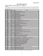
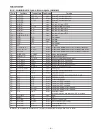
IC903~IC905 VHi-1: LED Driver (BU2114F)
• Outline
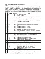
It is the low power consuming CMOS IC which has the latch in the 8-bit shift register and can asynchronously latch the data latched
in the shift register. Since the output (O1 to O8) is the open drain output (Since the protective diode is not provided, the voltage
of VDD or more to max. 7V is applicable, and the drive is possible at 36mA per output up to the total output of 150mA. (Static
operation mode)
1
SIN
Input
Serial data input terminal
2
CK
Input
Shift clock of shift register
3
LATCH
Input
When the terminal is turned to "L", the latch output is held.
Moreover, the latch output also varies as the shift register output varies when it is "H".
4*
SOUT
Output
Output of shift register of the final step
5
EN
Input
Enable terminal of O1 to O8
When the terminal is "L", the latch output appears as it is.
However, the output Qn is "L" when the latch output is "H", and Qn is "hi-Z" when the latch
output is "L".
6
RST
Input
Shift register, latch reset
7 - 9
GND
—
0V Power supply
10
O8
Output
Latch output at 8th step of shift register
11
O7
Output
Latch output at 7th step of shift register
12
O6
Output
Latch output at 6th step of shift register
13
O5
Output
Latch output at 5th step of shift register
14
O4
Output
Latch output at 4th step of shift register
15
O3
Output
Latch output at 3rd step of shift register
16
O2
Output
Latch output at 2nd step of shift register
17
O1
Output
Latch output at 1st step of shift register
18
VDD
—
+VDD power supply
Pin No.
Port Name
Input/Output
In this unit, the terminal with asterisk mark (*) is (open) terminal which is not connected to the outside.
Note) Output of O1 to O8 is an open-drain type, and when the output of the shift register is "H", the output becomes the level "L".
Function
SIN
CK
LATCH
SOUT
EN
RST
GND
GND
GND
V
DD
01
02
03
04
05
06
07
08
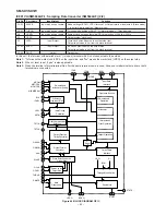
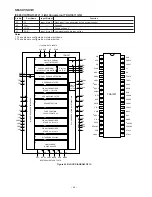
Figure 43 BLOCK DIAGRAM OF IC

