
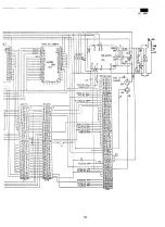
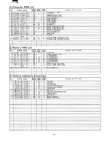
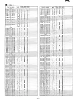
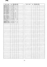
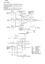


3. Description of each block
3-1. LR38045
gate array
Table below shows the functions
and port address of the
gate array block.
Block
Function
Bu
A bidirectional 8-bit Input/output buffer.
(8-bit 1/0 buffer)
Mu
Used to select FF1, FF2, FF3, or PA port
(multiplexer)
when data are read from the gate
arrav.
FF1~FF3
FF1:
The interrupt circuit is ControlIed with
(S-bit latch)
an FFl outpur. For instance, when a
certain bit is
set
to "1 ", the
Input
signal to the PA port (PAO~61
I
wh ich
corresponds to the bit is sent on the
IRQ llne as an interrupt signal.
FF2:
PB
port
(PSO~7Nllatch
FF3:
PC
port
(PCO~7Nllatch
DC1~3
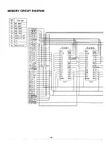
DCl : For generation of 32KS ROM chip
(decoder)
select signal. (CSNO)
DC2:
For generation of 2.5" FDD select
signal. (I07N)
DC3: For selection of FFl ~FF3 and FFD
reset latch at the time of data write.
Or selection of FFl ~FF3 or PA port
at the time of data read.
INT
Inputs to the PA port (PAO~611 are ORed
(Interrupt circuit)
and sent on the IRQ line as an interrupt
signal.
As PAO~61 correspond to QO~Q6 of FF1,
the i
nterrupt
is enabled when FF 1 is
set
with "1".
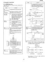
(Fig. 3 shows the quivalent circuit of the
interrupt circuit.)
IRQ
p
~
r;;;::-r-
QO
PAOI
QI
PAlI
Q2
PA21
Q8
PA81
Q4
PA.41
Q6
PAS I
Q6
PA61
'----
To multiplexer
(Fig. 3) Interrupt circuit
RST
FFl ~3 are reset by this
circuit,
when
a
reset
(reset circuitl
signal is received on RSTI.
At the same time, the 2/5" FDD reset signal
(RSTN) is issued which will be keot active
u ntil cleared by software.
_L....
-65-
-
PC-l600
Block
Function
It is possible without an input on RST! to
outpur RSTN by msans öf
sottware.
(Fig. 4 shows the equivalent circuit of the
reset
circuit and Fig. 5 shows its timings.)
R$TN
·RSTE.
'l1li1
0'"
[)o
I
I
•
IFrom
PC-1600)
~
..
FFl
-3
RESET
(Fig. 41 Reset circuit
JlSTE___n
~=============
OD.
RSTN
~
Software
reset
(Fig. 51 Reset circuit timings
CMT I/F
I
The cassette signal received from the EAR
(cassette
interface
jack is amplified and waveform
shaped,
circuitl
to be sent on PA78. (See Fig.6 for its
equivalent circuit.1
EAR----tl ..........
_.!. :
~
~
fU1Jl
.
.
~---------
-----------~
(Fig. 6) Cassette interface circuit equivalent
circuit
NOTE:
Ports, PA, PB, and PC, are all active high within
the gate arrav,
but they are converted
to active
low signals outside of the gate arrav,
Gate array
I
Inside
I
Outside
I
PAO-61
PBON~7N
PCON-7N
ACTIVE HIGH
AcTIVE
lOW
For
instance,
if "1"
is set to 00
of FF2, the
PBON outpur becomes low.
Содержание PC-1600
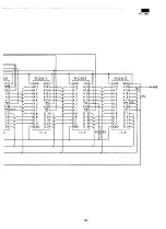
Страница 42: ... 11 CIRCUIT DIAGRAM PARTS POSITION KEY P W B LCD SIDE 39 ...
Страница 43: ...PC l600 40 ...
Страница 44: ...PC 1000 KEY P W B LSI SIDE 41 ...
Страница 45: ... 42 ...
Страница 48: ... PC l600 F P C P W B 45 ...
Страница 49: ... Kn 46 ...
Страница 52: ... PC l600 CONNECTOR P W B 49 ...
Страница 53: ... 50 ...
Страница 55: ... __ PC l600 tli I ONLY Pc 1600K I I 1 I 52 l J ...
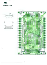
Страница 56: ... PC l600 K MEMORY P W B ROM Cut c IJ O lJ1F C O lJ1F I Bend capacitor to inward ROM SIDE 53 ...
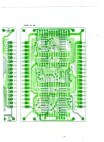
Страница 57: ...RAM SIDE 54 ...
Страница 61: ...I I 2 3 4 42 58 ...
Страница 92: ... PC l600 POWER SUPPLY P W B BACK VIEW MAIN P W B I Capacitor l00µF 10V mounting 20 25 tJ WB Oo 89 ...
Страница 93: ... P W B LSI SIDE t 90 ...
Страница 95: ... PC 1600 I rr 25 c oA C Screws are required torque control See service precation on section 6 page 69 93 ...
Страница 117: ... PC I600 ...


