background image


PARTS MARKED WITH 


 ARE IMPORTANT

MAINTAINING THE SAFETY OF THE SET. BE SURE TO RE-
PLACE THESE PARTS WITH SPECIFIED ONES FOR MAINTAIN-
ING THE SAFETY AND PERFORMANCE OF THE SET.

CAUTION:
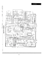
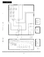
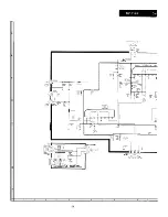
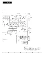
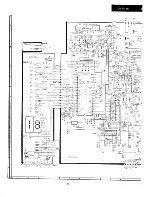
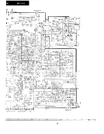
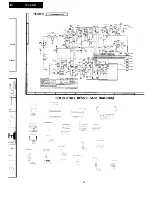
This circuit diagram is original one, therefore there may be a

slight difference from yours.
All the voltages in each point are measured with digital multi
meter.
All these figures represent the voltage levels measured upon
reception of colour signals.

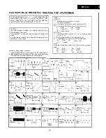
Waveform Measurement Conditions
1.

Upon receiving 

 colour bar signal of 70 

 in field intensity.

2. 

 indicates wave form check points (See chart, waveforms

and measured from point indicated to chassis ground).


NOTE:
RESISTOR

Resistance values are shown in ohms:
K= 7,000 M= 

All resistores are 

 watt, unless otherwise noted.

All resistores are Carbon, unless other wise noted.

 . . . . . . Solid

. . . . . .

Cement

 . . . . . .

Oxide Film

. . . . . . Special

. . . . . . Metal Coating

CAPACITOR

Capacitance values are shown in 


 otherwise noted


All capacitors are 

 unless otherwise noted.

All 

 are Ceramic, unless otherwise noted.

(ML) . . . . . . Mylar

. . . . . . . Polypro Film

(TA) . . . . . . . Tantalum

DIODE
Diode are, shown parts name other Diode are shown cathode
colour.

(BL) . .   BLUE

(BR) . . . . . . BLACK

. . . . . . YELLOW

 . . . . . . WHITE

. . . . . . GREEN

(OR) . . . . . . ORANGE

Содержание DV-5145

Страница 1: ...SSEMBLIES 17 l BLOCK DIAGRAMS 19 SCHEMATIC DIAGRAMS AND WAVEFORMS 21 l REPLACEMENT PARTS LIST 27 Aerial Input Impedance 75 ohm unbalanced Convergence Self Converging System Focus High Bi potential electrostatic Audio Power Output Rating 2W max Intermediate Frequencies Picture IF Frequency 36 875MHz Sound Carrier Trap 31 375MHz Adjacent Sound Carrier Trap 38 375MHz Powerlnput 240VAC50Hz Power Consu...

Страница 2: ...e at close range the following precautions should be observed 1 When repairing the circuit be sure not to increase the high voltage to more the 28kV at beam 1 l mA for the set 2 To keep the set in a normal operation be sure to make it function on 25 0kV 1 5 kV at beam 1 2 mA in the case of the set The set has been factory adjusted to the above mentioned high voltage If there is a possibility that ...

Страница 3: ...y using 10 key in combination with one of 1 to 6 keys 2 Pins arrangement of IClOl and its external connec tion 3 Key matrix Table l l Eo El E2 E3 I Fo F F2 F3 j F4 I 10 i I 4 8 FT 1 5 9 1 FT 6 2 T I 3 7 T F ICI101 rt wlOUTP T J VI 22 t 4 21 F5 4L j E vss 5v CLOCK vGG 30 20 Fe VHF f lc3 IL BAND OUTPlJT c AFT MUTE SOUND MUTE Figure l l 4 Sweeping speed of tuning key Table l 3 Tyew I TUNING I FINE TU...

Страница 4: ... voltage And when the key is touched off the data of tuning voltage is written in the memory When FT or FT key is pushed the unit performs a sweeping of tuning voltage And when the key is touched off the data of tuning voltage is written in the memon Within 2 seconds after 10 key has been pushed when one of 1 to 6 keys is pushed one of 11 to 16 positions is displayed but not tuned in since the dat...

Страница 5: ...UND SOUND IF INPUT Pin 0 AGC cut in level Pin 0 Generation of vertical sawtooth wave Pin 0 Vertical drive output Pin Vertical feedback circuit correction of vertical linearity and size Pin 0 Tuner RF AGC Pin PIF ground Pin 0 Power supply B 1 IV Pin IF input Pin IF input Pin I IF decoupling capacitor Pin 0 Sound volume control Pin 0 Audio output Pin 0 SIF detection Pin SIF decoupling capacitor Pin ...

Страница 6: ...ical output circuit 2 When the vertical drive circuit and vertical output circuit are in action it is only in the flyback period that the booster pump up circuit is allowed to operate to provide the voltage about twice Vcc 3I The design that the supply voltage is boosted only in the flyback period results in remarkably reduced power consumption 4 In the conventional SRPP output circuit Vcc must be...

Страница 7: ...of error amplifier 1 The voltage which is induced at N3 winding is DC rectified to produce a control voltage between pins and 0 The control voltage available at N3 is highly correla tive with the output voltage of N4 because both N3 and N4 are electrically coupled with each other 2 Variation of the control voltage is detected by TRl and ZDl 3 As the detec e voltage increases it is amplified by t d...

Страница 8: ...ck level clamping and burst keying Pin Video data switching Switching between R G B input and video input is performed R G B input at High level video input at Low level Pin I Luminance signal input Pin 0 Brightness control Pin 0 Red output Pin 8 Input of external red Pin I Green output Pin Input of external green Pin I Blue output Pin 0 Input of external blue Pin 0 Pin I Pin Black level clamping ...

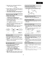
Страница 9: ...2V cm Connect a resistor 100 ohms to both ends of R229 10 kohms and short C Note Keep the lead of the 100 ohm resistor as short as possible AShorting __ L J T201 P DET 5 Apply DC voltage about 5V TP207 IF AGC and adjust so that the output waveform on oscilloscope is at O GVp p Note The voltage applied to TP207 should not ex ceed 7V in any case 6 Check that the overall waveform is within the speci ...

Страница 10: ... Screen control at MIN position l G bias control R853 A at MIN position l B bias control R853 B at MIN position l R bias control R869 at MIN position l G drive control R854 A at CENTER position l B drive control R854 B at CENTER position l Contrast control R 1110 at M IN position l Brightness control Rl 110 at CENTER position l Picture control R 1110 at CENTER position l Colour control Rl 110 at M...

Страница 11: ... picture is 5 mm higher than the geometrical center of CRT set S501 at down position If it is 5 mm lower than the geometrical center of CRT set S501 at up position D 5 mm or more t 5 mm or more d o w n h APC adjustment R802 Protector check 1 Receive luminance order colour bar signal 2 Short TP803 and TP804 and also TP801 and TP802 4 Remove the short circuits between TP803 and T804 3 Adjust R802 so...

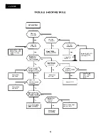
Страница 12: ...V line No Yes is normal _ r Check Q702 Check D502 0711 1 R741 T701 and 115 V line R725 Waveform at base of 0601 No 1 4 Check R724 I YCS I Q701 Q703 D710 and D716 I Check IC203 I I No Check R617 and T602 Yes c I HI 4 terminal No Check D709 and R732 gi No I Waveform at YCS TP403 is normal No I I 1 I I Check IC203 Q401 and A V Unit Check IC801 12 ...

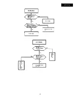
Страница 13: ...NO COLOUR I I No I YOS Check IC801 I I I No I I 1 I Check RlllOand R817 I I Check IC801 I NO PICTURE I YIK Check IC801 RlOOl Q40 1 and Video Switch Unit I Check Q850 0851 and Q852 IC203 Q203 and Tuner 13 ...

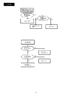
Страница 14: ...Waveform at No Check IC203 No w w 1 c k IC501 a n d Check L501 I I NO SOUND Yes Check IC201 0301 and IClOl Waveform at Yes c 4 No I Check IC301 1 1 I Check SP301 J3001 and L301 I 14 ...

Страница 15: ...3WE SPEAKER Sp301 j DNETo AF E UNJT 1 OT J Z REAR VIEW HEAD PHONE UNIT DUNTK4176WE H CENT u 601 j OIiOI m TP202 0 IC203 T201 L601 IF no CF401 Ill Il II lC2Ol u n 0203 0401 l u I r H SIZE cc all T301 II1 u T 302 7f 30 c501 0 TPZO 01 y J n lC3 Tf YJNER 0 TP2OI ISA II f iR7 f u IGJ c d R701 cl c XC701 Al C706 OL R707 L 0 T701 D 0 c719 1 ...

Страница 16: ...07 l 0 04008 0 04006 OJ 04005 0 rl IC4001 I I rJ 0 El I 4008 SUB SOUND IC4004 I I IC4003 01 0 I I DUNTK4172WE J40Ol J4003 J4002 h 11 AB3 0 ABI 0 s7001 J3OOl TA TB T 01107 5Cl l 6CH 7CH 8CH 9CH IOCH SllO5 SllO6 SllO7 SllO8 Silo9 SlllOl SIIII Slll2 S1113 S1114 q aiollollollollol m SllOl FINE TUNE I St103 TUNE I I 7 I 8 I 9 I 10 I 11 I 12 I 16 ...

Страница 17: ...ere are shown an viewed from their wiring sides J l z 4 I f 1 r I z C G I p J l l Jl I lo k j LCA N t 703 M R701 D O u ft 702 CA L706 c7cJ l D ow jl 2 4 I P R ma C6 5 t I i 3 4 56 kl r 4 E Mother Unit A B CRT Socket Unit 1 1 2 1 3 1 4 I 6 I 6 I 17 ...

Страница 18: ...5CEZZ oi EO Power Switch Unit R3002 3002 u N QPWBF4176CEZZ Earphone Jack Unit _ OPW8F41 3 EZZ _ Ta LEln5 J 5 3 DUNTK4173WE g 5 n 1 fj by 6 F ml 3 c 101 31 2 CCYTQAST c PlC W 6 d 51 01 I 1 5 c i O pq yijyf E q J q y 9 21115 51116 2 7 lT 1 SAN0 5E i ECT 5 v Control Unit 6 I 7 I 8 I 9 I 10 I 11 I 12 18 ...

Страница 19: ... G Hi E a a s E Y 0 9 m r F v x I E 1 t 0 I I I 3 II I I I I II I I 3 I I A L I 1 I 2 I 3 I 4 I 5 I 6 I 7 19 ...

Страница 20: ...E 3 c5ezld5 8 0 7 G 0 0 0 0 0 0 0 0 0 0 0 0 0 0 0 0 0 0 0 0 0 0 0 0 0 0 0 0 I I 2 E ti 0 0 0 z Fi r 0 z z 0 Z N 0 P o 0 ii ii In u l E l Z m ii Gl u Z I 5 ii v Gi IO 0 L __ _ a z o 3 3 0 I I m l II OQI Do lr7l II c I t OP t z cI 2 2 5 I 31 5 5 3 ii J s 2 zz a I 7 I 8 I 9 I 10 I 11 I 12 I 20 ...

Страница 21: ...E I 22 WF U6W IC4003 t AUDIO SW LA70 lb AVDIO IN c4020 L R4052 62K N I I 4050 8 OOK m r c4052 04005 01 lSSl19 tn IBL t A Dl0 Jr c4i 33 AA D4006 155119 BLl R4066 100 TO DWlX4167WE 7 1 2 FROU DuHT1 4173wE IOJ 1 I 2 I 3 I 4 I 6 I 6 I woo6 5K tll IC400 I TV VIDEO SW LA7C SVB SOWD 21 ...

Страница 22: ...8 15 Y 2SC I8 15 Y C4086 IO 116 AA 1 0 CXNTK 4 167WE WI 0 IX04 I6CE PC I406HA TJ YELLOW SERVICE PRECAUTION The area enclosed by this line is directly connected with AC Mains Voltage When servicing the area connect an isolating transformer between TV receiver and AC line to eliminate hazard of electric shock 6 I 7 I 0 I 9 I 10 I 11 I 12 1 22 ...

Страница 23: ...I DUNTK 74WE IOPWBF I74CEZZI j I i I tloj T 2 In _01 2 Iz A CT _ 1 1 joi j I i I i wz le16 s FT 9219 3L 4 u 1 1 DUNTK4 l87wE mPWEF4 lB7CEZZl 23 ...

Страница 24: ...950 j iz _ z 21 r J h l 10 0 J WI I 715 ZZOCE 2 501 FT 0 I 274CE 15 J 001 i 736 I 25 071 t DX0224cCE CmGP IOD 3 0 t117 220 3 tm I SAG 24 ...

Страница 25: ... dB in field intensity 2 m indicates wave form check points See chart waveforms and measured from point indicated to chassis ground I I 1 I 1 hhhC 17 h h j i zfl n f i i 1 h i lY n 1 NOTE RESISTOR 7 Resistance values are shown in ohms K 7 000 M 7 000 OOO 2 All resistores are l 8 watt unless otherwise noted 3 All resistores are Carbon unless other wise noted Solid Cement Oxide Film Special Metal Co...

Страница 26: ...j i j lP1456 891 5 SH IX0640CEiZ _ I c ii ii rrsr 1 1 IPJ4561 RH PX0164CEZZ J r 0 j _ 2 SZSD313F IE 3 13 yy ZZ1 56 8 3 Y i LI TIEI1 S25KJS4C0 COL LCTOII QMPTE0040CEZ SE c I iSZSCi 403R1E j I 3 V VI ii I JhiLL i23456 1 __ _ SZSCItl15CW I USCI9OCJTIE i S2511015 111E r I COLLECIOs j LW IFR 3 I I 4 J tl sc CoLLLCIO IY ITES 3 xs 6ZCE Z 1 YmLL i0 W i0a m 5 SC2 36 VYSCZZ I EIA I 3 2 ix 5 I y I L B Sf COI...

Страница 27: ...ZZ Degaussrng C o i l DIODES VHDlSSllSII 1 AB 201 301 404 601 717 722 806 D105 D106 D203 D204 801 DUNTK41 87WEV0 Mother Unit D U N T K 4 1 8 8 W E V 0 CRTUnit DUNTK41 7 2 W E V 0 A V Unit DUNTK4 17 3WEV0 Control Unit DUNTK41 74WEV0 LED Unit DUNTK41 75WEV0 Power Switch Unit DUNTK41 76WEV0 Earphone Jack Unit R H EX0020GEZZ Zener Diode AE RMPTJ0038CEZZ Zener Diode Pack AD R H EX0053TAZZ Zener Diode A...

Страница 28: ...47pH AF 732 L707 V P XFR33MOOOO 0 33pH AB 733 L801 V P CF390KOOOO 39pH AB 736 L807 V P XF6R8KOOOO 6 8gH AB c505 VCFYSB2AB104K 0 1 1 oov Mylar AC 808 c507 VCEAGAlVW227M 2 2 0 3 5 v Electrolytic AC 809 737 c509 VCSATAlVE105K 1 3 5 v T a n t a l u m A D c510 V C E A G A l V W 1 0 8 M 1 0 0 0 3 5 V Electrolytic AD C602 VCQPSA2AA272G 0 00271OOV Polypro AD Film CERAMIC FILTERS C603 R C QZA473TAYJ 0 0 4 ...

Страница 29: ...Z 3 9k 5 W CAPACITORS Cement AD R615 V R S VV3DB820J 8 2 2 W Oxide Film AA R617 C854 VRN VV3ABlR5J 1 5 IW VCKYPA2HB 102K 0 0 0 1 5 0 0 V Metal C e r a m i c A A AA C855 R C EZ0131TAZZ 1 0 250V Coating Electrolytic AD 9 R701 R R WZOO24CEZZ 6 8 7 W A C 8 5 6 R C KZ0023CEZZ 0 0 0 4 7 Cement AE C e r a m i c A D 1 R702 V R C UA2HGB25K 8 2M 112W Solid AA b 7 0 3 R707 R R WZ0063CEZZ 1 2 3 W Cement AB R7...

Страница 30: ... 1 1 1 4 fIs1115 yS1116 COILS L4001 VP CF151KOOOO 150 PH AB L4002 VP DF 1 OOKOOOO 10 LH AB L4003 VP CF681KOOOO 68 ItH AB 1 L7001 RCi LF0069CEZZ Line Filter AH DIODE D1201 R H PXOOl 1GEZZ L E D T V V I D E O AD CONTROL R4008 R V R B 5 1 3 7 C E Z Z 5k B Sub Sound AB CAPACITORS SWITCH C4008 VCEAGAl CW108M c4043 VCE9AAlCW226M s7001 Q S W P0370CEZZ Power Switch AK c4049 VCEAGAlCW337M h c7001 VCFYSK3AB...

Страница 31: ...3085CESA VI Indication Plate Hi ND M 2 4 6 5 C E S A Indicator inside the door BH AK AG AD AC AE REF NO PART NO DESCRIPTION H P N C 0133CESA J B T N 1 3 1 5 C E S A Punching Plate Button Channel CCABBl593WEVO Not Available H i NDP2291CEZZ LHLDW1007CEOO Back Cabinet Ass y Back Cabinet Indication Plate VIDEO AUDIO AC Cord Holder JKNBP1099CESA Knob Slide Control J B T N 1010CESA Button Mono Stereo J ...

Страница 32: ...S H A R P T5157 S MW KY ...

Отзывы: