CD-C471
l
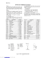
Resistor:
To differentiate the units of resistors, such symbol as and
are used: the symbol means 1000 ohm and the symbol
means 1000 kohm and the resistor without any symbol is
ohm-type resistor. Besides, the one with “Fusible” is a fuse
l
Capacitor:
To indicate the unit of capacitor, a symbol is used: this
symbol
means micro-micro-farad and the unit of the
capacitor without such a symbol is microfarad. As to
electrolytic capacitor, the expression “capacitance/withstand
voltage” is used.
(CH), (TH),
(UJ): Temperature compensation
(ML): Mylar type
(P.P.): Polypropylene type
l
Schematic diagram and Wiring Side of
for this
model are subject to change for improvement without prior
notice.
REF. NO
DESCRIPTION
POSITION
OPEN/CLOSE
TAPE
SW712
SW718
CENTER MODE/PHANTOM
CENTER MODE/NORMAL
SW721
DOLBY PRO LOGIC BYPASS
SW723
REC PAUSE
l
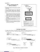
The indicated voltage in each section is the one measured
by Digital
between such a section and the chas-
sis with no signal given.
1. In the tuner section,
indicates AM
2. In the main section, a tape is being played back.
3. in the deck section, a tape is being played back.
indicates the record state.
4. In the power section, a tape is being played back.
5. In the CD section, the CD is stopped.
l
Parts marked with
are important for
maintaining the safety of the set. Be sure to replace these
parts with specified ones for maintaining the safety and
performance of the set.
SW801
VOLTAGE SELECTOR
1 1 0 - 1 2 7 -
SWM 3
REC FWD
REC RVS
SWM 5
SWM 6
CAM
E C B
268 GR
KTC3203
Figure 18 TYPES OF TRANSISTOR AND LED
Содержание CD-C471 W
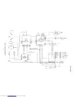
Страница 16: ... I I Ill I i c r __ __ I Figure 16 BLOCK DIAGRAM 2 3 16 ...
Страница 17: ...CD C471 W w UTER lC56115621563 N5M4558L lC562 1 2 Figure 17 BLOCK DIAGRAM 3 3 17 ...
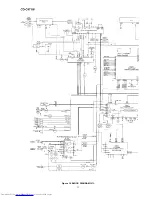
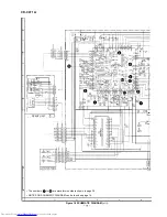
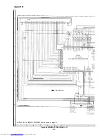
Страница 20: ...CD C471 W l NOTES ON SCHEMATIC DIAGRAM can be found on page 14 1 2 3 4 5 6 Figure 20 SCHEMATIC DIAGRAM 3 13 20 ...
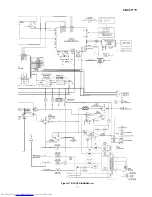
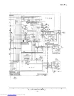
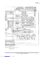
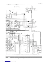
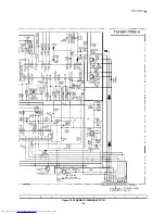
Страница 30: ...CD C471 W CD NORMAL REC OTHERCD NORMAL PLAY I 2 I 3 I 4 5 6 Figure 30 SCHEMATIC DIAGRAM 13 l 3 30 ...
Страница 31: ...CD C471 W 1 SWICH PWB A3 1 DISPLAY PWB A2 1 7 8 9 10 11 12 I Figure 31 WIRING SIDE OF P W BOARD l E 3 1 ...
Страница 36: ... POWER PWB B 1 MAII IUPWB P33 7 A 1 2 3 4 5 6 Figure 36 WIRING SIDE OF P W BOARD 6 8 36 ...
Страница 54: ...CD C471 W MEMO 54 ...
Страница 66: ...CD C471 W 620 12 614x2 hy2 x b16 226 L 235 234 609x2 611 236 SOLM2 1 2 3 4 5 6 CABINET EXPLODED VIEW 2 2 ll ...
Страница 69: ...CD C471 W WOOFER SPI L CH SP2 R CH SPI 2 904 1 I 2 I 3 I 4 I 5 I 6 SPEAKER EXPLODED VIEW 2 2 14 ...
Страница 70: ......
Страница 71: ...CD C471 W MEMO ...


